Silicon Wafer Reclaim & Reprocessing Market Research Report –Segmentation by Wafer Diameter (100 mm, 150 mm, 200 mm, 300 mm, Others); by Reprocessing Service Type (Polished Wafer Reclaim, Test Wafer Reclaim, Prime Wafer Reclaim, Grinding / Lapping / Etching Reprocessing, Others); by Wafer Type (Bare Silicon Wafers, Epitaxial Wafers, Patterned Wafers, Monitor Wafers, Others); by End Use (Process Stage, Equipment Qualification & Calibration, Process Monitoring, R&D and Pilot Line, Test and Inspection, Others) ; and Region - Size, Share, Growth Analysis | Forecast (2026– 2030)
Global Silicon Wafer Reclaim & Reprocessing Market Size (2026-2030)
In 2025, the Silicon Wafer Reclaim & Reprocessing Market was valued at approximately USD 610 million. It is projected to grow at a CAGR of around 4.2% during the forecast period of 2026–2030, reaching an estimated USD 749.32 million by 2030.
The Global Silicon Wafer Reclaim and Reprocessing Market is the community of technology, service vendors, and operational methodologies devoted to reclaiming used semiconductor wafers for use again in manufacturing industries. It aims at reusing silicon wafers that have already gone through fabrication or testing, or monitoring processes, and reusing them for non-production purposes. The market includes surface treatment, polishing, cleaning, grinding, and other precision processes that rehabilitate wafer functionality as well as lengthen lifecycle value. It is used by the semiconductor manufacturers to decide on cost efficiency, sustainability, and continuity of operations in the fabrication environments.
This market also has the reclaim and refurbishment services that are used on the used wafers in the semiconductor fabrication sites. It normally includes the process of wafer recovery of engineering experiments, equipment tests, inspection schedules, and process validation activities at fabrication plants. It, however, excludes the fabrication of newly fabricated prime wafers or raw silicon substrates that are the by-products of crystal growth activities. Rather, it focuses on circular utilization in semiconductor manufacturing settings, in which reclaimed wafers are a dependable and economical substitute for non-critical functional needs.
In recent years, the environment has been changing as the demand and supply of semiconductors have been changing, with increased sustainability commitment and manufacturer-supply chain volatility across chip manufacturing. Semiconductor fabs have given reclaim strategies a lot of priority in order to minimize wastage of materials and maximize the rate of wafer utilization. Improved surface restoration technology, automated polishing processes, and greater control of contamination of reclaimed wafers have made reclaimed wafers suitable for a wider variety of process monitoring and development activities.
Key Market Insights
It is estimated that, month by month, 300 mm wafer manufacturing will be approximately 9.6 million wafers, increasing the reclaim demand.
Fabrication facilities of semiconductors are expensive (up to 20 billion dollars) and promote solutions to cost-effective wafer reuse.
Over 70 percent of semiconductor manufacturing today depends on 300 mm wafers, which raises the reclaim volumes worldwide.
Greater investment in semiconductor ecosystems is being accelerated as governments around the world anticipate more than 400 billion US dollars in semiconductor incentives between 2023 and 2027.
The investment funds in China alone for semiconductors exceeded 190 billion dollars in various national programs, which reinforced regional wafer supply chains.
To be competitive, semiconductor manufacturers are forced to keep utilization rates at 85 percent and more, which means more test-wafer reuse studies.
The use of AI-based server semiconductors will increase by approximately 11.6 percent per year, making it challenging to test and optimize processes on the wafer.
Approximately 60 percent of all technology COOs around the world are weighing reshoring manufacturing footprints and rearchitecturing regional wafer processing ecosystems.
Circular wafer reuse efforts are reinforced by electronics supply chains that produce 65-80% of lifecycle emissions in the manufacturing of components.
Research Methodology
Scope & Definitions
Defines the Silicon Wafer Reclaim & Reprocessing Market as commercial services that restore used semiconductor wafers for reuse in testing, monitoring, and R&D.
Includes reclaim services for bare, epitaxial, patterned, and monitor wafers across 100–300 mm diameters; excludes new wafer manufacturing and unrelated semiconductor materials processing.
Global scope with historical review, current baseline, and forecast horizon defined in-report.
Segmentation follows wafer diameter, service type, wafer type, process stage, and geography using a standardized data dictionary.
Double counting prevented by locking measurement to the service transaction layer and allocating revenue to a single segment only.
Evidence Collection (Primary + Secondary)
Primary interviews across reclaim service providers, semiconductor fabs, equipment vendors, and materials distributors.
Expert consultations with process engineers, procurement leaders, and fab operations specialists.
Secondary evidence from company disclosures, technical publications, semiconductor industry reports, and relevant regulators/standards bodies/industry associations specific to Silicon Wafer Reclaim & Reprocessing Market (named in-report).
The report uses verifiable sources and provides source-linked evidence supporting key claims.
Triangulation & Validation
Market sizing built through bottom-up service revenue aggregation and top-down semiconductor wafer utilization benchmarks.
Reconciliation against company financial disclosures and capacity indicators.
Conflicting sources resolved through multi-source comparison and expert validation.
Presentation & Auditability
All assumptions, formulas, and segment allocations documented in a transparent model framework.
Tables, charts, and forecasts supported by source-linked evidence for auditability and enterprise decision use.
Increased Volumes in Semiconductor Manufacturing and the Necessity of Cost Reduction.
The semiconductor market is growing all over the world as digital technology has penetrated almost all sectors of the modern economy. Semiconductor demand is at an all-time high as electric cars and advanced driver assistance systems are becoming more popular, cloud computing is gaining acceptance, and industrial automation is being driven by consumer electronics. Since the fabrication factories expand production to drive this demand, the consumption level of silicon wafers will grow exponentially. It is in this respect that wafer reclamation and reprocessing services have become one of the necessary operational approaches of semiconductor manufacturers that aim to attain cost-efficiency, as well as long-term sustainable production.
Increasing Sustainability and Circular Manufacturing Focus in Semiconductor Manufacturing.
The concept of sustainability has taken center stage in the entire electronics sector in the world. The semiconductor production, being technologically sophisticated, is also resource-consuming, using large quantities of both energy and water and raw materials. With the ever-increasing environmental regulations and the promise of corporate sustainability, semiconductor manufacturers are turning to circular manufacturing approaches with increasing numbers. In this change, the reclaim and reprocessing service of wafers is very important.
Growing Test and Monitor Wafer Requirements in State-of-the-Art Semiconductor Processes.
The increasing market of test, monitor, and equipment qualification wafers utilized in silicon fabrication processes is also another significant market catalyst of the silicon wafer reclaim and reprocessing market. The current state of semiconductor manufacturing demands constant surveillance and calibration to achieve accuracy at nanometer production scales. The demand for stable process control wafers has grown tremendously as the architecture of the devices has grown in complexity. In the manufacturing of semiconductors, multiple process procedures are to be thoroughly reviewed before production wafers are sold.
Although there is an increasing interest in cost-effective wafer reuse, the silicon wafer reclaim and reprocessing market has a number of hurdles in its operations and technology. It requires highly accurate cleaning, polishing, and defect removal, which adds complex cost and processing to the process and precludes scalability in some suppliers. Moreover, there are high semiconductor manufacturing standards that tend to limit the number of times semiconductor wafers can be reused without loss of yield. Quick changes in wafer and device architectures also pose a challenge to the reclaim providers, as the plant has to constantly upgrade the equipment and skills to suit the industry requirements.
The increasing volumes of semiconductor fabrication are providing opportunities to wafer reclaim and reprocessing vendors. Manufacturers of foundries and devices are increasingly exploring cost-effective mechanisms of reusing wafers in testing, equipment calibration, and pilot production. The increase in sustainability requirements also promotes recycling and material recovery in fabs. In the meantime, the high-speed technology scaling is widening the demand for reclaimed wafers in the process monitoring and research and development process. The companies providing service-enhancing precision reprocessing, reducing turnaround time, and handling advanced wafer formats will be in a good position to seize high opportunities as fabs focus on both efficiency and environmental care in their operation.
How this market works end-to-end
The silicon wafer reclaim and reprocessing ecosystem follows a workflow closely tied to semiconductor fabrication operations.
Wafer usage inside the fab
Semiconductor fabs use silicon wafers not only for production but also for monitoring processes, qualifying equipment, and running pilot experiments.
Collection of used wafers
After process monitoring, inspection, or equipment calibration cycles, used wafers accumulate within fabrication facilities.
Sorting by wafer diameter
Used wafers are grouped by diameter categories such as 100 mm, 150 mm, 200 mm, and 300 mm. Diameter matters because reclaim methods must match handling equipment and polishing tolerances.
Classification by wafer type
The wafers are also categorized by structure. Bare silicon wafers, epitaxial wafers, patterned wafers, and monitor wafers require different reprocessing methods.
Selection of reclaim service
Reprocessing providers apply different services depending on wafer condition. Common services include polished wafer reclaim, test wafer reclaim, prime wafer reclaim, and grinding, lapping, or etching processes.
Surface restoration and inspection
Reclaim operations remove thin material layers, eliminate contamination, and restore surface quality so wafers can be reused in monitoring environments.
Quality validation
Reprocessed wafers undergo inspection to confirm flatness, thickness uniformity, and surface quality.
Redistribution for fab processes
Reclaimed wafers return to semiconductor facilities where they support process monitoring, equipment qualification, R&D pilot lines, and inspection procedures.
What matters most when evaluating claims in this market
Claim type
What good proof looks like
What often goes wrong
Market size assumptions
Clear separation between reclaim services and new wafer production
Counting wafer manufacturing revenue as reclaim activity
Technology capability
Evidence of compatibility with multiple wafer types and diameters
Overstating capabilities across all wafer formats
Process coverage
Clear mapping to fab activities like monitoring or equipment qualification
Generic claims about “semiconductor demand”
Supply dynamics
Analysis tied to fab utilization and process monitoring needs
Treating reclaim demand as consumer electronics demand
Service differentiation
Detailed description of reclaim methods and inspection standards
Marketing language without process detail
The decision lens
Confirm the market boundary
Ensure the report measures reclaim services only and excludes wafer manufacturing.
Check the wafer diameter coverage
Reports should clearly analyze 100 mm, 150 mm, 200 mm, and 300 mm wafers.
Compare reclaim service categories
Different services address different wafer conditions and fab needs.
Evaluate wafer type coverage
Bare silicon, epitaxial, patterned, and monitor wafers should be treated separately.
Examine process stage usage
The report should show how reclaimed wafers support equipment calibration, monitoring, R&D, and inspection.
Review geographic coverage
Global analysis should reflect the distribution of semiconductor fabrication activity.
The contrarian view
A common mistake in this market is treating wafer reclaim demand as a direct reflection of semiconductor chip demand. In reality, reclaim services are tied more closely to fab operations.
Another issue is boundary confusion. Some analyses include wafer manufacturing revenue alongside reclaim services, which inflates estimates and distorts comparisons.
Hidden double counting also occurs when the same wafers are counted multiple times across process stages. Proper analysis tracks reclaim activity at the service transaction level.
Finally, many reports assume that all wafer diameters grow equally. In practice, reclaim demand often concentrates around specific wafer sizes aligned with active fabrication infrastructure.
Practical implications by stakeholder
Semiconductor fabrication facilities
Optimize operating costs by reusing wafers for monitoring and calibration tasks.
Evaluate reclaim providers based on wafer diameter compatibility and process precision.
Wafer reclaim service providers
Differentiate services through polishing quality and wafer type capabilities.
Align service capacity with dominant wafer formats used in semiconductor fabs.
Semiconductor equipment manufacturers
Design equipment compatible with reclaimed wafers used in testing and calibration.
Track wafer reclaim trends to anticipate process monitoring needs.
Semiconductor materials distributors
Coordinate wafer supply chains where reclaimed wafers supplement new wafers for testing environments.
Research and development labs
Use reclaimed wafers to reduce experimentation costs while maintaining process consistency.
Silicon Wafer Reclaim & Reprocessing Market – By Wafer Diameter
Introduction/Key Findings
100 mm
150 mm
200 mm
300 mm
Others
Y-O-Y Growth Trend & Opportunity Analysis
The reason is the share of 300 mm wafer diameter, which is the highest at about 52, which is the most sought after in the advanced semiconductor manufacturing, where the high-volume production uses large-size wafers because it is efficient and economical. The use of 300 mm fabs worldwide in the chip production centers has continued to reinforce the demand for reclaimed wafers in the process testing and calibration activities.
The fastest-growing segment is the 200 mm wafer segment, which has almost a 24 percent share, assisted by the rising legacy fabs manufacturing analog, power, and automotive chips. The ongoing use of specialty semiconductors, in addition to the renewal of older fabrication lines, is influencing the continuous increase in the reclaimed 200 mm wafers for testing and monitoring, and pilot production lines.
Silicon Wafer Reclaim & Reprocessing Market – By Reprocessing Service Type
Introduction/Key Findings
Polished Wafer Reclaim
Test Wafer Reclaim
Prime Wafer Reclaim
Grinding / Lapping / Etching Reprocessing
Others
Y-O-Y Growth Trend & Opportunity Analysis
Services that are polished wafer reclaim have the highest percentage of about 38 percent because the semiconductor fabs use polished reclaimed wafers to regain surface flatness and eliminate layers of contamination. These wafers find extensive application in the alignment of lithography, equipment configuration, and non-production testing, which allows manufacturers to save on operational costs.
The fastest growing segment with a share percentage of around 22 is the grinding, lapping, and etching reprocessing services due to the demand for precise wafer surface conditioning in high semiconductor nodes. The demand for specialized surface treatment services in semiconductor manufacturing facilities is increasing because of increased demands for complex fabrications and a decrease in process tolerances.
Silicon Wafer Reclaim & Reprocessing Market – By Wafer Type
Introduction/Key Findings
Bare Silicon Wafers
Epitaxial Wafers
Patterned Wafers
Monitor Wafers
Others
Y-O-Y Growth Trend & Opportunity Analysis
Silicon Wafer Reclaim & Reprocessing Market – By End Use Process Stage
The market is dominated by the Asia Pacific at approximately 46 percent, which is backed by robust ecosystems in China, Taiwan, South Korea, and Japan in semiconductor manufacturing. There is a concentration of wafer fabrication plants in the region, which has led to high demand for reclaimed wafers to be used in equipment qualification, process calibration, and production monitoring.
The fastest-growing region is North America, which has almost a 24% share due to increased investments in semiconductors and local production of chip projects. Europe is contributing close to 17% as a result of high production of automotive semiconductors, South America with almost 7%, and the Middle East and Africa with almost 6%, because they are emerging technology markets and are slowly gaining momentum.
Latest Market News
Jan 18, 2026: A semiconductor equipment company in the world and a reclaim inspection company announced a strategic alliance to design automated reclaim inspection systems. The joint venture aims to achieve 30% reduced wafer qualification cycles by 2027 to assist fabs interested in achieving greater reuse of monitor and test wafers.
Oct 09, 2025: A large semiconductor materials manufacturer announced a new wafer reprocessing line that can reclaim defects of up to 40 on a 300 mm wafer with an improved yield of the wafer in process monitoring applications. The plant should help the semiconductor global customers in excess of 500,000 reclaimed wafers each year.
June 3, 2025: A semiconductor recycling company acquired a Taiwanese regional wafer reclaim company and reinforced its presence in the Asia-Pacific region. The acquisition broadens service offerings in three more fabs and more than 25 percent of reclaim throughput.
Feb 14, 2025: A European wafer reclaim firm said it had upgraded its technology to provide superior polishing methodologies that can then lengthen wafer reuse lifespan to 5-8 reclaims and minimize material wastage in semiconductor fabrication facilities. Initial experiments showed an 18 percent reduction in the cost of wafer procurement in pilot-line processes.
Sep 22, 2024: A semiconductor materials consortium has introduced a joint reuse program related to circular wafer reuse strategies, with the goal of increasing the level of reclaim adoption by 35 percent by 2028. It is a project that incorporates over 12 semiconductor makers and suppliers of materials in Asia, Europe, and North America.
May 07, 2024: A wafer reclaim technology firm has launched a high-precision metrology system that is 22 times more accurate in defect detection and allows fabs to use reclaimed wafers in more challenging process-monitoring schemes. There were four semiconductor fabs where the solution was first rolled out.
Jan 16, 2024: A semiconductor materials supplier based in the world declared an enlargement of their reclaim services offering, including assisting advanced-node patterned wafers applied in equipment testing. The program was projected to raise the demand for reclaim services by 19 percent in 2024 pilot deployments in several fabrication sites.
Key Players
Nova Electronic Materials
Kemi Silicon Inc.
Silicon Quest International
Rockwood Wafer Reclaim
Silicon Valley Microelectronics Inc.
Silicon Materials Inc.
Shinryo Corporation
Phoenix Silicon International Corporation
Optim Wafer Services
Pure Wafer
Questions buyers ask before purchasing this report
What exactly does the Silicon Wafer Reclaim & Reprocessing Market measure?
The market measures commercial services that restore used semiconductor wafers so they can be reused inside fabrication facilities. These services include polishing, grinding, and surface restoration processes that remove contamination or thin damaged layers. The focus is on reclaim operations rather than wafer manufacturing. Reports typically analyze reclaim services by wafer diameter, service type, wafer structure, process stage, and geography.
Why are reclaimed wafers important for semiconductor fabs?
Reclaimed wafers help semiconductor fabs reduce operational costs. Instead of using expensive production wafers for equipment calibration or monitoring processes, fabs can reuse reclaimed wafers for these tasks. This approach preserves new wafer supply for production while maintaining consistent process control and testing routines.
How do wafer diameter trends influence reclaim demand?
Wafer diameter determines both processing equipment and fab infrastructure. Reclaim services must match the wafer sizes used in active fabrication environments. As fabs transition between wafer formats or maintain multiple diameter generations, reclaim providers must support those specific wafer categories.
What types of wafers are typically reclaimed?
Several wafer types can be reclaimed depending on the fabrication process. Bare silicon wafers are common candidates. Epitaxial wafers, patterned wafers, and monitor wafers can also undergo reclaim procedures when surface conditions allow reprocessing. Each wafer type requires different treatment methods during the reclaim cycle.
Where are reclaimed wafers used inside semiconductor fabrication?
Reclaimed wafers are typically used in non-production process stages. Common applications include equipment qualification, process monitoring, inspection routines, and R&D experiments. These tasks require wafers with consistent geometry but do not require pristine production quality.
How should buyers evaluate the credibility of a reclaim market report?
Buyers should confirm that the report clearly defines its market boundary and excludes wafer manufacturing revenues. Strong reports also explain reclaim service categories, wafer diameter coverage, wafer type classification, and fab process usage. Transparent segmentation and operational workflow analysis help ensure accurate market interpretation.
Does reclaim demand follow semiconductor industry cycles?
Reclaim demand does relate to semiconductor activity, but the relationship is indirect. Reclaim services depend on fab utilization, process monitoring intensity, and equipment calibration routines. These operational factors can differ from consumer electronics demand cycles.
What insights should a decision-grade market report provide?
A strong report should map reclaim services to semiconductor fab operations, analyze wafer diameter and wafer type dynamics, and explain how reclaim services support monitoring and testing environments. It should also provide a clear geographic view of semiconductor fabrication capacity.
To Learn more about this report,
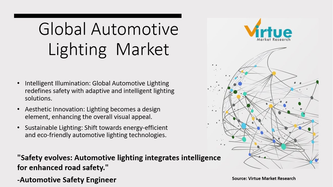
Global automotive lighting refers to all vehicle lighting systems, from headlamps that illuminate the road to taillights that communicate movements. They guarantee motorists and other road users alike safety, visibility, and style. While taillights frequently use LEDs for improved visibility, headlights are available in a variety of technologies, including LED and laser. Interior illumination, DRLs, and signal lights all have a role to play. This market, which was estimated to be worth $33.64 billion in 2022, is anticipated to rise to $67.39 billion by 2030 because of laws, luxury tastes, safety concerns, and technological developments like OLED taillights and adaptive headlights. Anticipate a future dominated by intelligent, connected, personalized, and sustainable lighting systems that enhance the safety, efficiency, and aesthetic appeal of automobiles.
Key Market Insights:
Car lighting works its magic to provide safety, visibility, and style. Headlights cut through the night, taillights express intent, and interiors shine with comfort. The billion-dollar global business is expected to rise due to consumer demand for high-end experiences, safer roads, and cutting-edge technology. Imagine dynamic messages being painted by taillights, headlights that adjust to the road, and interiors that customize their atmosphere. Driven by technological advancements like linked systems and laser beams, this future is calling. Anticipate even more visually attractive, environmentally friendly, and intelligent lighting to illuminate the way ahead, making cars safer, more efficient, and unquestionably cooler.
Global Automotive Lighting Market Drivers:
Using cutting-edge technology to illuminate the road, safety serves as a guiding light.
In the market for automobile lighting, safety is the driving force behind demand from the public and laws. While automated high beams smoothly react to traffic, adaptive headlights modify their beams so as not to blind other people. With visually striking displays, dynamic taillights convey intentions for braking and turning. Beyond these developments, integrated pedestrian identification and lane departure alerts will soon make roads safer and brighter for everyone.
Beyond Performance-Based Luxuries Redefined by Light.
Luxurious automobile lighting creates a distinct visual identity that goes beyond simple illumination. Personalized interior lighting customizes the driving experience by setting the mood with a range of colours and intensities, while intricate designs and distinctive DRLs modify exteriors. As you approach your automobile at night, welcoming lights lead the way, resulting in an interior that is perfectly lit. Not only is this symphony of light aesthetically pleasing, but it also stands as a tribute to luxury. Upcoming developments like gesture-controlled lighting and holographic displays promise to further enhance the experience.
Fuel Efficiency Takes the Lead: Illuminating Sustainability
The worldwide automotive lighting market is undergoing a significant transition towards energy-efficient solutions, as environmental concerns gain prominence. LED technology is leading the way, providing a ray of hope for the environment and drivers alike. LED lights beam brighter and use a lot less energy than conventional halogen lamps. There are some tangible advantages to this. For drivers, this translates to increased fuel economy, which lowers petrol prices and lessens reliance on fossil fuels. Greater air quality and a reduction in the transport sector's contribution to climate change are the results of reduced overall emissions.
To Learn more about this report,
Global Automotive Lighting Market Restraints and Challenges:
Although the global automotive lighting business is booming, there are still unknowns. Difficulties impede growth even as innovation propels it with eye catching features like laser beams and adaptable headlights. These technologies are luxury items due to their high cost and difficult integration, which puts producers' abilities to the test. The worldwide patchwork created by unclear legislation limits the potential of innovation. Durability issues persist, particularly when complex systems are subjected to challenging conditions. Ultimately, a lot of drivers still don't fully understand how these improvements can help them. Together, we can overcome these obstacles. The keys to reducing costs are improved production, more seamless integration, and unified regulations. Their full potential can be realized by educating customers about the safety, efficiency, and aesthetic value of these lighting wonders. By working together, we can pave the way for an even brighter and safer future for vehicle lighting.
Global Automotive Lighting Market Opportunities:
It is made possible by advanced LED technology, which gives drivers the ability to customize their illumination for the highest level of comfort and flair. Consumers that care about the environment want greener products, and vehicle lighting complies. While solar- and self-powered lighting technologies offer a future powered by clean energy, energy-efficient LEDs lower pollution. The advent of connected lighting systems heralds a new age. Envision automobiles interacting with infrastructure and one another to minimize accidents and enhance traffic efficiency. Integrated headlights with pedestrian recognition provide unmatched safety, while dramatic taillights with eye-catching displays alert onlookers to your intentions. The possibilities are endless in the future. Gesture-controlled interior illumination, holographic displays projected onto the road, and even light fixtures with self-healing capabilities.
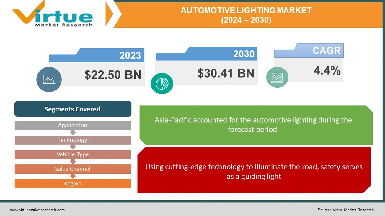
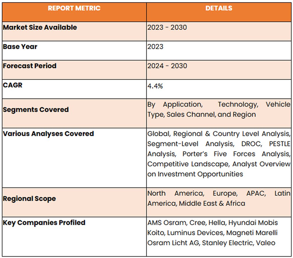
AUTOMOTIVE LIGHTING MARKET REPORT COVERAGE:
To Learn more about this report,
Global Automotive Lighting Market Segmentation: By Application
Exterior Lighting
Interior Lighting
Due to laws requiring safety features like headlights, taillights, and brake lights, exterior lighting presently holds the most market share in the vehicle lighting industry. The dominance of this market is partly attributed to advancements in safety-focused technologies such as adaptive headlights and daytime running lights. The market value of external lighting is increased by the quick adoption of technology like LED bulbs and laser lights, which improve performance and aesthetics. Conversely, the interior lighting market is expected to increase at the fastest rate in the upcoming years. Innovations like ambient lighting and technology breakthroughs like LED and OLED displays, driven by consumer demand for comfort and personalisation, open new possibilities. The spread of sophisticated interior lighting systems is further driven by the growing emphasis on safety and the expansion of the luxury car market.
Global Automotive Lighting Market Segmentation: By Technology
Halogen
LED (Light-Emitting Diode)
Xenon
Emerging Technologies
The worldwide vehicle lighting market is currently dominated by halogen because of its more affordable price, advanced technology, and useful illumination. With its dependable supply chain and affordable option for manufacturers and cost-conscious customers, halogen holds the biggest market share. The fastest-growing market right now is LEDs, which are predicted to shortly overtake halogen. The rapid expansion of LEDs is driven by their higher efficiency, longer lifespan, flexibility in design, and technological breakthroughs including enhanced brightness. Because LEDs use less energy and produce fewer emissions and better fuel economy, they are becoming more and more popular in the changing automotive lighting market.
Global Automotive Lighting Market Segmentation: By Vehicle Type
Passenger Cars
Commercial Vehicles
Passenger automobiles rule the worldwide automotive lighting market. The sheer number of passenger cars produced which surpasses that of business vehicles and fuels the need for lighting systems is the primary cause of this popularity. The growing demand for personal automobiles in developing nations is a result of rising disposable income, which in turn drives the rise of the passenger car market. The importance that consumers place on safety and aesthetics elements helps to drive market expansion. But in the upcoming years, the market for electric and hybrid cars is expected to develop at the quickest rate. The exponential rise of the worldwide electric car market, which is still expanding and shows no signs of slowing down, is what is driving this surge. Specialised lighting solutions are required since electric and hybrid vehicles have different lighting requirements because of their specific functionality and design aesthetics.
Global Automotive Lighting Market Segmentation: By Sales Channel
OEM (Original Equipment Manufacturers)
Aftermarket
Most lighting systems sold nowadays are sold by OEMs (Original Equipment Manufacturers), primarily because manufacturers pre-install lighting systems in new cars. But in the next years, the aftermarket is expected to develop at the quickest rate. This spike in demand for replacement parts, especially lighting systems, can be linked to several variables, one of them being the average age of cars. The industry is expanding because of consumers' growing desire to personalise their cars with aftermarket lighting upgrades such LED upgrades and decorative lighting. The availability and affordability of technologies like adaptive headlights and laser lights in the aftermarket, together with other advancements in lighting technology, are driving demand even more. Moreover, the growing market for electric cars (EVs).
To Learn more about this report,
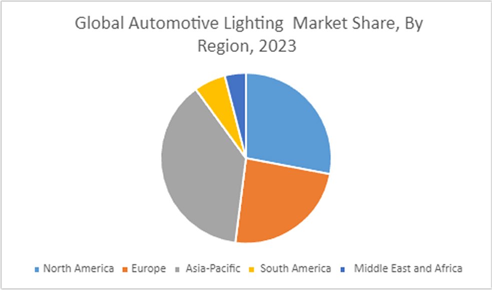
Global Automotive Lighting Market Segmentation: By Region
North America
Asia-Pacific
Europe
South America
Middle East and Africa
Throughout the forecast period, Asia Pacific is anticipated to be the automotive lighting market with the highest profitability. Over the past few years, Asia Pacific countries like China and India have seen notable increases in automotive manufacturing and sales, primarily in the medium-to premium luxury car segment. Asia Pacific is predicted to see an increase in the manufacturing of passenger cars, with India experiencing the strongest growth rate. Depending on the state of the national economy, the area offers a suitable selection of both high-end and cheap cars. For instance, there is a substantial demand for halogen, Xenon/HID, and LED since China and India produce more economy and mid-range automobiles. On the other hand, luxury car adoption rates are greater in South Korea and Japan, where LED lighting is the norm.
COVID-19 Impact Analysis on the Global Automotive Lighting Market:
A brief shadow was thrown by COVID-19 over the worldwide automotive lighting market. Production was stopped by lockdowns and supply chain disruptions, while luxury lighting upgrades were shelved by consumers on a tight budget. Resources became scarce, and R&D stagnated. Still, the market is recovering thanks to resurgent demand and rearranged priorities. While energy-efficient LEDs are being pushed towards adoption by sustainability, safety concerns are driving interest in features like pedestrian detection and adaptive headlights. The digital push of the epidemic creates opportunities for intelligent, networked lighting systems that may interact with infrastructure and other cars. Ultimately, the industry is positioned to shine brighter, focused on safety, sustainability, and a connected future, even though the pandemic dimmed its brilliance.
Recent Trends and Developments in the Global Automotive Lighting Market:
A development collaboration between OSRAM Continental and REHAU aims to incorporate lighting into external components, providing automobile manufacturers with innovative lighting options that improve functionality and design flexibility. For rear combination lamps, Hella unveiled a revolutionary lighting innovation called Hella FlatLight technology. A Memorandum of Understanding (MoU) was signed by Samvardhana Motherson Automotive Systems Group BV (SMRPBV), a division of Motherson Group, and Marelli Automotive Lighting to investigate a technology collaboration focused on intelligently lighted external body components. Valeo debuted their revolutionary 360° lighting system at the Shanghai Auto Show. This technology surrounds the car with a band of light, projecting instantaneous, clear signs that other drivers can see from a distance. Pedestrians, cyclists, and scooter riders are especially susceptible to these signals
Key Players:
AMS Osram
Cree
Hella
Hyundai Mobis
Koito
Luminus Devices
Magneti Marelli
Osram Licht AG
Stanley Electric
Valeo
Chapter 1. Silicon Wafer Reclaim & Reprocessing Market– Scope & Methodology
1.1. Market Segmentation
1.2. Scope, Assumptions & Limitations
1.3. Research Methodology
1.4. Primary Wafer Type `
1.5. Secondary Source Chapter 2. Silicon Wafer Reclaim & Reprocessing Market– Executive Summary
2.1. Market Size & Forecast – (2026 – 2030) ($M/$Bn)
2.2. Key Trends & Insights
2.2.1. Demand Side
2.2.2. Supply Side
2.3. Attractive Investment Propositions
2.4. COVID-19 Impact Analysis Chapter 3. Silicon Wafer Reclaim & Reprocessing Market– Competition Scenario
3.1. Market Share Analysis & Company Benchmarking
3.2. Competitive Strategy & Development Scenario
3.3. Competitive Pricing Analysis
3.4. Supplier-Distributor Analysis Chapter 4. Silicon Wafer Reclaim & Reprocessing Market- Entry Scenario
4.1. Regulatory Scenario
4.2. Case Studies – Key Start-ups
4.3. Customer Analysis
4.4. PESTLE Analysis
4.5. Porters Five Force Model
4.5.1. Bargaining Power of Suppliers
4.5.2. Bargaining Powers of Customers
4.5.3. Threat of New Entrants
4.5.4. Rivalry among Existing Players
4.5.5. Threat of Substitutes Chapter 5. Silicon Wafer Reclaim & Reprocessing Market- Landscape
5.1. Value Chain Analysis – Key Stakeholders Impact Analysis
5.2. Market Drivers
5.3. Market Restraints/Challenges
5.4. Market Opportunities
Chapter 6. Silicon Wafer Reclaim & Reprocessing Market– By Wafer Diameter
6.1 Introduction/Key Findings
6.2 100 mm
6.3 150 mm
6.4 200 mm
6.5 300 mm
6.6 Others
6.7 Y-O-Y Growth trend Analysis By Wafer Diameter
6.8 Absolute $ Opportunity Analysis By Wafer Diameter , 2026-2030
Chapter 7. Silicon Wafer Reclaim & Reprocessing Market– By Reprocessing Service Type
7.1 Introduction/Key Findings
7.2 Polished Wafer Reclaim
7.3 Test Wafer Reclaim
7.4 Prime Wafer Reclaim
7.5 Grinding / Lapping / Etching Reprocessing
7.6 Others
7.7 Y-O-Y Growth trend Analysis By Reprocessing Service Type
7.8 Absolute $ Opportunity Analysis By Reprocessing Service Type 2026-2030
Chapter 8. Silicon Wafer Reclaim & Reprocessing Market– By End Use Process Stage
8.1 Introduction/Key Findings
8.2 Equipment Qualification & Calibration
8.3 Process Monitoring
8.4 R&D and Pilot Line
8.5 Test and Inspection
8.6 Others
8.7 Y-O-Y Growth trend Analysis End Use Process Stage
8.8 Absolute $ Opportunity Analysis End Use Process Stage , 2026-2030 Chapter 9. Silicon Wafer Reclaim & Reprocessing Market– By Wafer Type
9.1 Introduction/Key Findings
9.2 Bare Silicon Wafers
9.3 Epitaxial Wafers
9.4 Patterned Wafers
9.5 Monitor Wafers
9.6 Others
9.7 Y-O-Y Growth trend Analysis Wafer Type
9.8 Absolute $ Opportunity Analysis, Wafer Type 2026-2030
Chapter 10. Silicon Wafer Reclaim & Reprocessing Market, By Geography – Market Size, Forecast, Trends & Insights
10.1. North America
10.1.1. By Country
10.1.1.1. U.S.A.
10.1.1.2. Canada
10.1.1.3. Mexico
10.1.2. By Wafer Diameter
10.1.3. By Wafer Type
10.1.4. By End Use Process Stage
10.1.5. Reprocessing Service Type
10.1.6. Countries & Segments - Market Attractiveness Analysis
10.2. Europe
10.2.1. By Country
10.2.1.1. U.K.
10.2.1.2. Germany
10.2.1.3. France
10.2.1.4. Italy
10.2.1.5. Spain
10.2.1.6. Rest of Europe
10.2.2. By Wafer Diameter
10.2.3. By Wafer Type
10.2.4. By End Use Process Stage
10.2.5. Reprocessing Service Type
10.2.6. Countries & Segments - Market Attractiveness Analysis
10.3. Asia Pacific
10.3.1. By Country
10.3.1.2. China
10.3.1.2. Japan
10.3.1.3. South Korea
10.3.1.4. India
10.3.1.5. Australia & New Zealand
10.3.1.6. Rest of Asia-Pacific
10.3.2. By Wafer Diameter
10.3.3. By Reprocessing Service Type
10.3.4. By End Use Process Stage
10.3.5. Wafer Type
10.3.6. Countries & Segments - Market Attractiveness Analysis
10.4. South America
10.4.1. By Country
10.4.1.1. Brazil
10.4.1.2. Argentina
10.4.1.3. Colombia
10.4.1.4. Chile
10.4.1.5. Rest of South America
10.4.2. By Reprocessing Service Type
10.4.3. By Wafer Diameter
10.4.4. By Wafer Type
10.4.5. End Use Process Stage
10.4.6. Countries & Segments - Market Attractiveness Analysis
10.5. Middle East & Africa
10.5.1. By Country
10.5.1.4. United Arab Emirates (UAE)
10.5.1.2. Saudi Arabia
10.5.1.3. Qatar
10.5.1.4. Israel
10.5.1.5. South Africa
10.5.1.6. Nigeria
10.5.1.7. Kenya
10.5.1.10. Egypt
10.5.1.10. Rest of MEA
10.5.2. By Wafer Diameter
10.5.3. By Reprocessing Service Type
10.5.4. By End Use Process Stage
10.5.5. Wafer Type
10.5.6. Countries & Segments - Market Attractiveness Analysis Chapter 11. Silicon Wafer Reclaim & Reprocessing Market – Company Profiles – (Overview, Portfolio, Financials, Strategies & Developments)
11.1 Nova Electronic Materials
11.2 Kemi Silicon Inc.
11.3 Silicon Quest International
11.4 Rockwood Wafer Reclaim
11.5 Silicon Valley Microelectronics Inc.
11.6 Silicon Materials Inc.
11.7 Shinryo Corporation
11.8 Phoenix Silicon International Corporation
11.9 Optim Wafer Services
11.10 Pure Wafer
Fill out the form below and our team will get back to you shortly
FAQ's
The Global Silicon Wafer Reclaim & Reprocessing Market was valued at approximately USD 610 million in 2025 and is projected to reach an estimated USD 749.32 million by the end of 2030. Over the forecast period of 2026–2030, the market is projected to grow at a CAGR of around 4.2%.
Rapid expansion of semiconductor fabrication plants, increasing complexity of semiconductor manufacturing processes, and the need for strict contamination control in chip production are major drivers of the Global Silicon Wafer Reclaim & Reprocessing Market. In addition, rising investments in semiconductor supply chain resilience and localization initiatives are accelerating demand for wafer reuse and reclaim services across semiconductor fabrication facilities.
. 100 mm, 150 mm, 200 mm, 300 mm, and Others are the segments under the Global Silicon Wafer Reclaim & Reprocessing Market by Wafer Diameter.
Asia-Pacific is the most dominant region for the Global Silicon Wafer Reclaim & Reprocessing Market.
Nova Electronic Materials, Kemi Silicon Inc., Silicon Quest International, Rockwood Wafer Reclaim, Silicon Valley Microelectronics Inc., Silicon Materials Inc., Shinryo Corporation, Phoenix Silicon International Corporation, Optim Wafer Services, Pure Wafer, RS Technologies Co., Ltd., Kinik Company, Scientech Corporation, TOPCO Scientific, and Mimasu are key players in the Global Silicon Wafer Reclaim & Reprocessing Market.
More related reports
Get expert-driven market research reports from a leading research partner to help you navigate the future of the global industry.
Report Code: VMR-19367 | Published Date: May 2026 | Format: Excel and PDF
As of 2025, the market was estimated to be around USD 410 billion, which took into account the cumulative investments, production, and development of the ecosystem associated with the localized production of semiconducto...
Report Code: VMR-19286 | Published Date: April 2026 | Format: Excel and PDF
In 2025, the global Nearshoring and Contract Manufacturing for Electronics Market was valued at approximately USD 759.93 billion. It is projected to grow at a CAGR of around 12.66% during the forecast period of 2026–2030...
Report Code: VMR-19221 | Published Date: March 2026 | Format: Excel and PDF
In 2025, the High-Temperature Electronics Market was valued at approximately USD 3.94 billion. It is projected to grow at a CAGR of around 7% during the forecast period of 2026–2030, reaching an estimated USD 5.53 billio...
Report Code: VMR-19228 | Published Date: March 2026 | Format: Excel and PDF
In 2025, the Semiconductor Probe Cards Market was valued at approximately USD 2.6 billion. It is projected to grow at a CAGR of around 7.2% during the forecast period of 2026–2030, reaching an estimated USD 3.68 billion...
Report Code: VMR-19218 | Published Date: March 2026 | Format: Excel and PDF
In 2025, the Semiconductor Wafer Handling & AMHS Market was valued at approximately USD 6.2 billion. It is projected to grow at a CAGR of around 8.6% during the forecast period of 2026–2030, reaching an estimated USD 9.3...
“We received a complex piece of work for our niche market from Virtue Market research in short period of time. I appreciate the quality and content of the final files we received. Thanks for the support”
Medical Devices Company based in Europe
“We received a complex piece of work for our niche market from Virtue Market research in short period of time. I appreciate the quality and content of the final files we received. Thanks for the support”
Medical Devices Company based in Europe
“We received a complex piece of work for our niche market from Virtue Market research in short period of time. I appreciate the quality and content of the final files we received. Thanks for the support”
Medical Devices Company based in Europe
“We received a complex piece of work for our niche market from Virtue Market research in short period of time. I appreciate the quality and content of the final files we received. Thanks for the support”
Medical Devices Company based in Europe
“We received a complex piece of work for our niche market from Virtue Market research in short period of time. I appreciate the quality and content of the final files we received. Thanks for the support”
Medical Devices Company based in Europe
“We received a complex piece of work for our niche market from Virtue Market research in short period of time. I appreciate the quality and content of the final files we received. Thanks for the support”