GaN Epitaxy Wafers Market Size (2026–2030)
The GaN Epitaxy Wafers Market was valued at approximately USD 0.92 Billion in 2025 and is projected to reach a market size of around USD 2.85 Billion by the end of 2030. Over the forecast period of 2026–2030, the market is expected to grow at a CAGR of about 25.3%.
The GaN Epitaxy Wafers Market is gaining importance within the compound semiconductor industry due to the increasing demand for high-performance electronic and optoelectronic devices. Gallium nitride (GaN) is a wide-bandgap semiconductor material known for its high electron mobility, high breakdown voltage, and ability to operate at high temperatures. These properties allow GaN devices to deliver superior efficiency and performance compared with conventional silicon-based semiconductors.
Epitaxial wafers are semiconductor wafers formed through epitaxial growth processes in which a crystalline layer is deposited on a substrate to create high-quality semiconductor materials for device fabrication. These wafers are widely used in photonics, microelectronics, and advanced semiconductor manufacturing.
GaN epitaxy wafers are used extensively in power electronics, RF communication devices, LEDs, and laser diodes. The increasing demand for efficient power conversion technologies, high-frequency communication systems, and energy-efficient lighting solutions is driving strong demand for GaN materials. GaN epitaxial wafers are widely applied in fast chargers, power converters, 5G base stations, and defense radar systems due to their high efficiency and power output capabilities.
Furthermore, semiconductor manufacturers are exploring different substrate materials such as silicon carbide, sapphire, silicon, and native GaN to improve wafer performance and reduce production costs. As industries increasingly transition toward high-efficiency semiconductor technologies, GaN epitaxy wafers are expected to play a crucial role in next-generation power electronics and communication infrastructure.

Key Market Insights
- GaN materials offer higher power density and switching speeds compared with traditional semiconductor materials.
- GaN enables higher efficiency power electronics compared with silicon. Wide-bandgap materials such as GaN provide higher breakdown voltage, improved switching speed, and reduced energy losses in power electronic systems.
- GaN power electronics reduce system size and energy losses. Engineering studies show GaN-based systems can significantly reduce power loss while improving performance in advanced power conversion applications.
- Increasing demand for high-efficiency power electronics is accelerating the adoption of GaN semiconductor devices.
- Telecommunications infrastructure, particularly 5G base stations, relies heavily on GaN-based RF devices.
- Substrate innovations such as GaN-on-silicon technology are improving production scalability and reducing manufacturing costs.
- Asia-Pacific dominates semiconductor manufacturing and remains the largest production hub for GaN wafers.

Research Methodology
Scope & Definitions
- Defines the market boundary as product-level sales of GaN epitaxy wafers used in semiconductor device fabrication; excludes downstream device manufacturing and unrelated semiconductor materials.
- Covers global markets with regional analysis and a historical–forecast timeframe aligned with industry reporting cycles.
- Segmentation follows wafer size, substrate type, device type, end-use industry, and region, ensuring MECE classification with an “Others” category where needed.
- A structured data dictionary and classification rules standardize terminology and prevent double counting across segments.
Evidence Collection (Primary + Secondary)
- Primary research: interviews with wafer manufacturers, semiconductor device producers, distributors, and industry consultants across the value chain.
- Secondary research: company filings, technical papers, investor presentations, trade publications, and databases from relevant regulators/standards bodies/industry associations specific to GaN epitaxy wafers (named in-report).
- Key insights are supported with verifiable sources and source-linked evidence referenced directly within the report.
Triangulation & Validation
- Market size estimated using bottom-up analysis of supplier revenues and shipment volumes and top-down validation from semiconductor industry indicators.
- Results reconciled with company financial disclosures, capacity data, and demand-side indicators.
- Conflicting inputs are resolved using multi-source comparison, interview validation, and bias-control checks.
Presentation & Auditability
- Findings are presented with transparent assumptions, traceable data tables, and source citations for critical claims.
- Each dataset is cross-referenced to original sources, enabling verification and repeatability.
- The report structure ensures decision-grade clarity, reproducibility, and audit-ready documentation for enterprise stakeholders.

Market Drivers
The growing demand for High-Efficiency Power Electronics is driving the market
One of the most significant drivers of the GaN Epitaxy Wafers Market is the increasing demand for high-efficiency power electronics. GaN semiconductor devices enable higher switching frequencies and reduced energy losses compared with silicon-based power devices. These advantages make GaN materials ideal for power conversion applications such as electric vehicle charging systems, renewable energy inverters, and industrial motor drives. As industries seek to improve energy efficiency and reduce power consumption, the demand for GaN-based semiconductor technologies continues to increase.
Expansion of High-Frequency Communication Technologies is driving the market
Another key growth driver is the rapid expansion of high-frequency communication technologies such as 5G networks and satellite communications. GaN RF devices offer superior performance in high-frequency applications due to their high electron mobility and power density. These devices are widely used in telecommunications infrastructure, radar systems, and defense electronics, creating strong demand for GaN epitaxy wafers used in RF semiconductor manufacturing.
Market Restraints
Despite strong growth potential, the GaN Epitaxy Wafers Market faces several challenges. One major challenge is the high manufacturing cost associated with GaN wafer production. Producing high-quality epitaxial layers requires advanced crystal growth technologies and specialized semiconductor equipment, which increases production costs. Additionally, the availability of suitable substrates for GaN epitaxy remains limited. While sapphire and silicon substrates are widely used, each substrate material presents technical challenges such as thermal mismatch and defect formation. These challenges can affect wafer quality and production efficiency.
Market Opportunities
The increasing adoption of electric vehicles and renewable energy technologies presents major opportunities for the GaN Epitaxy Wafers Market. GaN power devices are increasingly used in electric vehicle power converters and fast-charging systems due to their superior efficiency and thermal performance. Furthermore, the growing deployment of 5G networks and next-generation communication infrastructure is expected to boost demand for GaN RF devices. As semiconductor manufacturers continue to improve epitaxial growth technologies and expand wafer production capacity, GaN materials are likely to gain broader adoption across multiple industries.
How this market works end-to-end
- Substrate preparation begins the process. Manufacturers start with base materials such as silicon carbide, sapphire, silicon, or native GaN substrates. Each option offers different thermal and electrical properties.
- Epitaxial growth forms the functional layer. Advanced techniques deposit thin GaN layers on the substrate. These layers determine device performance characteristics.
- Wafer size selection affects production economics. Manufacturers produce wafers in sizes such as 2-inch, 4-inch, 6-inch, and increasingly 8-inch formats.
- Quality inspection ensures device reliability. Defect density, crystal quality, and thickness uniformity are tested before wafers move forward.
- Device manufacturers purchase epitaxy wafers. These buyers produce power devices, RF components, or optoelectronic devices depending on design requirements.
- Fabrication converts wafers into semiconductor chips. Device fabrication facilities process the wafers through lithography, etching, and metallization steps.
- Chips move to industry-specific applications. Consumer electronics, telecom infrastructure, automotive systems, and industrial electronics use these devices.
- Regional manufacturing hubs shape supply chains. Semiconductor clusters influence where wafers are produced and where device manufacturing occurs.
What matters most when evaluating claims in this market
|
Claim type
|
What good proof looks like
|
What often goes wrong
|
|
Manufacturing capability
|
Evidence of wafer size production, yield consistency, and process maturity
|
Marketing claims that ignore yield challenges
|
|
Cost advantages
|
Clear explanation of substrate choice and scale economics
|
Oversimplified comparisons without process context
|
|
Performance improvements
|
Device-level testing tied to wafer quality
|
Claims based only on laboratory results
|
|
Market demand signals
|
Alignment with real semiconductor manufacturing trends
|
Overreliance on projected applications
|
|
Supply capacity
|
Transparent production expansion plans
|
Confusing wafer capacity with chip output
|
The decision lens
- Define the transaction boundary. Confirm that the report measures epitaxy wafer sales rather than downstream devices or system revenues.
- Compare substrate strategies. Examine how different substrates affect cost, thermal performance, and manufacturing scalability.
- Evaluate wafer size transitions. Determine whether suppliers are moving toward larger wafers and whether yields support commercial production.
- Assess demand drivers. Identify which device categories—power, RF, or optoelectronic—are shaping wafer demand.
- Review regional production clusters. Semiconductor ecosystems influence supply stability and manufacturing investment.
- Check consistency across segments. Ensure the report uses clear segmentation that avoids overlapping categories.
The contrarian view
Many analyses of the GaN epitaxy wafers market blur the line between materials and devices. This creates inflated market estimates because wafer sales and device revenues are counted together.
Another common mistake is assuming that larger wafers automatically lower costs. In reality, yield challenges and equipment upgrades can offset theoretical cost savings.
There is also a tendency to generalize demand across industries. Power electronics, RF devices, and optoelectronics each have different adoption timelines. Treating them as one demand pool hides important differences in technology maturity.
Finally, some reports treat substrate technologies as interchangeable. Each substrate changes manufacturing complexity, performance outcomes, and the economics of scaling production.
Practical implications by stakeholder
Semiconductor material suppliers
- Must invest in advanced epitaxy processes to reduce defects and improve yield.
- Strategic decisions around substrate technology shape long-term competitiveness.
Device manufacturers
- Need reliable wafer suppliers to maintain production consistency.
- Substrate selection directly influences device efficiency and reliability.
Electronics OEMs
- Performance expectations for power and RF components affect supplier choices.
- Supply chain stability becomes critical for large production programs.
Automotive manufacturers
- Power electronics efficiency is central to electrification strategies.
- Reliability requirements place strict demands on wafer quality.
Telecommunications infrastructure providers
- High-frequency RF performance depends on advanced semiconductor materials.
- Long-term supplier partnerships help secure component availability.
GaN EPITAXY WAFERS MARKET REPORT COVERAGE:
|
REPORT METRIC
|
DETAILS
|
|
Market Size Available
|
2024 - 2030
|
|
Base Year
|
2024
|
|
Forecast Period
|
2025 - 2030
|
|
CAGR
|
25.3%
|
|
Segments Covered
|
By Wafer Size, Substrate Type, Device Type, End-Use Industry and Region
|
|
Various Analyses Covered
|
Global, Regional & Country Level Analysis, Segment-Level Analysis, DROC, PESTLE Analysis, Porter’s Five Forces Analysis, Competitive Landscape, Analyst Overview on Investment Opportunities
|
|
Regional Scope
|
North America, Europe, APAC, Latin America, Middle East & Africa
|
|
Key Companies Profiled
|
WOLFSPEED, IQE PLC, SOITEC, EPIGAN, SUMITOMO ELECTRIC, NXP SEMICONDUCTORS, INFINEON TECHNOLOGIES, STMICROELECTRONICS, TOSHIBA CORPORATION, ROHM SEMICONDUCTOR
|
GaN Epitaxy Wafers Market Segmentation
GaN Epitaxy Wafers Market – By Wafer Size
|
- Introduction/Key Findings
- 2-inch
- 4-inch
- 6-inch
- 8-inch
- Others
- Y-O-Y Growth Trend & Opportunity Analysis
The 4-inch wafer segment currently dominates the GaN epitaxy wafers market due to its widespread use in commercial semiconductor manufacturing. Many GaN-based devices, including LEDs and RF components, are produced using 4-inch wafers because they offer a balance between production cost and device performance.
The 6-inch wafer segment is expected to be the fastest-growing category as semiconductor manufacturers transition toward larger wafers to improve production efficiency and reduce manufacturing costs.
GaN Epitaxy Wafers Market – By Substrate Type
- Introduction/Key Findings
- Silicon Carbide (SiC)
- Sapphire
- Silicon (Si)
- Gallium Nitride (GaN) Native Substrate
- Others
- Y-O-Y Growth Trend & Opportunity Analysis
GaN Epitaxy Wafers Market – By Device Type
- Introduction/Key Findings
- Power Devices
- RF Devices
- Optoelectronic Devices
- Others
- Y-O-Y Growth Trend & Opportunity Analysis
Power devices represent the largest segment in the market due to the growing use of GaN power electronics in energy conversion systems, fast chargers, and electric vehicles.
RF devices are expected to grow rapidly due to the increasing deployment of high-frequency communication technologies such as 5G infrastructure and satellite communication systems.

GaN Epitaxy Wafers Market – By End-Use Industry
- Introduction/Key Findings
- Consumer Electronics
- Telecommunications & Networking
- Automotive
- Industrial & Power Electronics
- Aerospace & Defense
- Others
- Y-O-Y Growth Trend & Opportunity Analysis

GaN Epitaxy Wafers Market – By Region
• North America
• Europe
• Asia Pacific
• Latin America
• Middle East & Africa
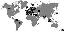
Asia-Pacific dominates the GaN Epitaxy Wafers Market due to its strong semiconductor manufacturing ecosystem and large electronics production base. Countries such as China, Japan, South Korea, and Taiwan host many semiconductor fabrication facilities and GaN device manufacturers.
North America is expected to be the fastest-growing region due to increasing investments in semiconductor manufacturing, expansion of 5G infrastructure, and rising demand for advanced power electronics technologies.
Key Players
- Wolfspeed
- IQE PLC
- Soitec
- EpiGaN
- Sumitomo Electric
- NXP Semiconductors
- Infineon Technologies
- STMicroelectronics
- Toshiba Corporation
- ROHM Semiconductor
Latest Market News
November 10, 2025 — GlobalFoundries signs GaN technology licensing agreement with TSMC
GlobalFoundries entered a technology licensing agreement with TSMC covering 650 V and 80 V gallium nitride technologies, expanding access to GaN-based power semiconductor manufacturing.
April 10, 2025 — IQE and X-FAB announce GaN power device platform collaboration
Compound semiconductor wafer supplier IQE and specialty foundry X-FAB signed a joint development agreement to create a European GaN power device platform to accelerate commercialization of GaN semiconductor technologies.
February 18, 2026 — GaN HEMT epitaxial wafer demand rises with RF and power electronics growth
Industry developments show growing demand for GaN HEMT epitaxial wafers driven by the expansion of high-frequency communication infrastructure and advanced power electronics applications.
Questions buyers ask before purchasing this report
What exactly does the GaN epitaxy wafers market measure?
The market measures the commercial supply of gallium nitride epitaxial wafers used in semiconductor manufacturing. It focuses on the material layer before device fabrication begins. The report excludes finished semiconductor devices and downstream electronics products. This boundary matters because wafer revenue represents a smaller but critical portion of the overall semiconductor value chain.
Why are substrate choices so important in this market?
The substrate forms the base on which GaN layers are grown. Different substrates affect thermal conductivity, electrical performance, and manufacturing complexity. Silicon carbide often supports high-performance devices, while sapphire and silicon offer cost advantages in some applications. Understanding substrate differences helps buyers evaluate supplier strategies and cost structures.
How do wafer sizes influence market dynamics?
Wafer size affects production economics. Larger wafers allow more devices to be fabricated per wafer, which can reduce manufacturing cost per chip. However, larger wafers also require advanced equipment and process control. Yield losses can offset potential savings, making the transition to larger wafers a complex industry decision.
Which industries are driving demand for GaN epitaxy wafers?
Demand primarily comes from industries that require high-efficiency or high-frequency semiconductor devices. Consumer electronics, telecommunications infrastructure, automotive systems, and industrial electronics all rely on advanced semiconductor components. Each industry adopts the technology at different speeds depending on cost and performance requirements.
Why is it difficult to estimate the true size of this market?
Market estimates become inaccurate when analysts mix wafer supply with downstream device revenues. These two layers of the semiconductor value chain represent different transaction points. Accurate analysis requires strict boundaries that measure wafer production and sales independently from device manufacturing.
What should buyers compare when evaluating different market reports?
Buyers should check how the report defines the market boundary, how it segments wafer types and substrates, and whether the methodology separates wafer supply from device production. They should also review how the report handles regional manufacturing differences and whether the analysis reflects real semiconductor supply chain structures.
How does regional manufacturing influence this market?
Semiconductor ecosystems tend to cluster geographically. Regions with strong fabrication infrastructure often drive demand for epitaxy wafers. These clusters influence supply chain logistics, investment decisions, and technology development. Understanding regional manufacturing patterns helps buyers anticipate shifts in supply and demand.