Gallium Arsenide (GaAs) Wafers Market Research Report –Segmentation by Wafer Type (Semi-Insulating (SI) GaAs Wafers, Semi-Conducting (SC) GaAs Wafers, Others); By Diameter (2-Inch, 3-Inch, 4-Inch, 6-Inch & Above, Others); By Polishing Type (Single-Side Polished (SSP), Double-Side Polished (DSP), Epi-Ready, Others); By End-Use Application (RF & Wireless Communications, Photovoltaics & Space Solar, Photonics & Optoelectronics, LED & Display, Defense & Aerospace, Others); and Region - Size, Share, Growth Analysis | Forecast (2026– 2030)
Global Gallium Arsenide (GaAs) Wafers Market Size (2026-2030)
The Gallium Arsenide (GaAs) Wafers Market was valued at USD 1.47 Billion in 2025 and is projected to reach a market size of USD 2.89 Billion by the end of 2030. Over the forecast period of 2026–2030, the market is projected to grow at a CAGR of 14.48%.
Gallium arsenide occupies an irreplaceable niche within the semiconductor substrate landscape that no amount of silicon engineering has been able to fully replicate. As a III-V compound semiconductor, GaAs offers electron mobility approximately five times higher than silicon, a direct bandgap that enables efficient light emission and absorption, and a semi-insulating substrate option that allows microwave and millimeter-wave devices to operate without the parasitic substrate losses that plague silicon-based RF designs. These properties are not incremental advantages; they are fundamental material characteristics that define why GaAs wafers remain the substrate of choice across an expanding set of high-frequency, high-efficiency, and optoelectronic applications despite decades of competitive pressure from silicon and newer compound semiconductors.
The GaAs wafer market bifurcates cleanly along electrical type. Semi-insulating (SI) GaAs wafers, produced by controlling the Fermi level through chromium doping or native defect engineering in liquid-encapsulated Czochralski (LEC) or vertical gradient freeze (VGF) growth processes, form the substrate platform for RF and microwave device fabrication. Semi-conducting (SC) GaAs wafers, doped with silicon or zinc to produce n-type or p-type conductivity, serve as the foundation for epitaxial LED, laser diode, and photovoltaic device growth. This bifurcation creates two structurally distinct demand streams with different growth drivers, customer profiles, and pricing dynamics within the same market boundary.
The RF and wireless communications segment has historically been the largest demand driver for SI GaAs wafers, sustained by the ubiquitous presence of GaAs pseudomorphic high-electron-mobility transistors (pHEMT) and heterojunction bipolar transistors (HBT) in smartphone power amplifiers, WiFi front-end modules, and satellite ground terminal transceivers. The transition to 5G handsets has intensified this demand, as 5G RF front-end architectures require more GaAs-based power amplifier and low-noise amplifier die per device than their 4G predecessors.
Key Market Insights:
According to McKinsey, the global semiconductor market reached about $775 billion in 2024 and could grow to $1.6 trillion by 2030, driven by AI, high-performance computing, and advanced connectivity technologies—applications that heavily rely on compound semiconductors such as GaAs for RF and optoelectronic devices.
Semiconductor demand is projected to grow dramatically, with the industry expected to approach $1.6 trillion by 2030, expanding opportunities for specialized materials like GaAs wafers used in RF and optoelectronic devices.
4-inch diameter wafers represented the largest volume production format in 2025, accounting for approximately 48% of total GaAs wafer shipments, as the majority of established RF and optoelectronic compound semiconductor fabs operate on 4-inch production platforms.
Epi-ready polished wafer surface specifications commanded a price premium of approximately 18 to 25% over standard single-side polished (SSP) wafers in 2025, reflecting the critical surface preparation requirements for high-quality epitaxial layer growth on photovoltaic and LED device substrates.
The photovoltaics and space solar segment expanded by approximately 22% year-on-year in 2025, driven by accelerating commercial satellite constellation deployment and growing government investment in space-based solar power feasibility programs requiring multi-junction GaAs cell substrates.
6-inch GaAs wafer adoption grew by approximately 31% in unit shipments during 2025, as leading RF device manufacturers transitioned select high-volume pHEMT power amplifier programs to larger diameter substrates to achieve die-per-wafer economics compatible with smartphone market pricing requirements.
Defense and aerospace applications accounted for approximately 14% of total GaAs wafer consumption in 2025, concentrated in phased-array radar, electronic warfare receiver modules, and secure satellite communications chip programs requiring radiation-tolerant GaAs substrates.
Research Methodology
1. Scope & Definitions
Boundary: sellable revenue from GaAs substrate wafers at the polished or epi-ready stage; excludes epitaxial wafers with device-specific grown layers, GaAs-based finished chips, and non-GaAs III-V substrate materials.
Segmentation: Wafer Type, Diameter, Polishing Type, End-Use Application, Geography; MECE with ‘Others’ buckets; single transaction layer (product sales revenue).
Data dictionary defines wafer revenue by diameter and type, crystal growth method classification, and double-counting prevention via manufacturer-level de-duplication across direct and distributor channels.
2. Evidence Collection (Primary + Secondary)
Primary interviews across the value chain: GaAs crystal growers, wafer manufacturers, epitaxy service providers, RF device IDMs, photovoltaic cell producers, and space systems integrators.
Secondary sources: SEMI substrate shipment statistics, IEA space solar publications, 3GPP 5G device specification data, NASA and ESA satellite program documentation; relevant regulators/standards bodies/industry associations specific to Gallium Arsenide (GaAs) Wafers Market (named in-report). All key claims carry verifiable, source-linked evidence.
3. Triangulation & Validation
Bottom-up sizing from GaAs wafer manufacturer shipment data and area-based consumption modeling; top-down modeling from RF front-end module market spend and satellite solar cell production volumes.
Reconciliation to disclosed financial filings, conflicting-source resolution, and expert re-validation for decision-grade accuracy.
4. Presentation & Auditability
Transparent assumptions ledger, cited exhibits, reproducible calculation steps, version-controlled datasets, and anonymized interview logs for full audit-grade traceability.
Market Drivers:
The global rollout of 5G networks and the proliferation of multi-band RF front-end modules in smartphones are sustaining structurally elevated demand for semi-insulating GaAs wafers used in pHEMT power amplifiers and HBT chipsets.
Every 5G-capable smartphone requires a significantly higher count of GaAs-based power amplifier die than its 4G predecessor, as multi-band carrier aggregation, sub-6GHz and millimeter-wave co-existence, and WiFi 6E integration each demand additional RF front-end components. Leading smartphone OEMs shipping hundreds of millions of units annually translates this per-device increase directly into sustained high-volume GaAs wafer demand. This demand vector is reinforced by the ongoing global base station densification that keeps infrastructure-grade GaAs MMIC procurement elevated in parallel with handset-driven consumption.
The accelerating deployment of commercial satellite constellations and growing government investment in space-based power generation are creating a structurally expanding demand vector for high-efficiency multi-junction GaAs solar cell substrates.
Low-Earth orbit commercial broadband constellations are deploying thousands of satellites annually, each requiring GaAs multi-junction photovoltaic panels as the primary power source given their unmatched space-grade efficiency above 30%. Simultaneously, several national space agencies and defense programs are funding feasibility studies and initial hardware for space-based solar power concepts that would require GaAs cell production at scales exceeding any prior space application. These independent programs converge to create a durable and growing demand floor for high-quality SC GaAs epi-ready wafers serving photovoltaic applications.
Market Restraints and Challenges:
The primary restraint is the structural competition from gallium nitride on silicon carbide substrates in the RF power amplifier market, where GaN-on-SiC HEMTs deliver superior power density and thermal performance at the power levels required for base station and defense electronic warfare applications. As GaN device economics improve with increasing production scale, a portion of the RF applications market that historically required GaAs substrates is migrating to GaN platforms, creating a competitive displacement risk at the higher power end of the RF device spectrum that constrains the addressable volume for SI GaAs wafers.
Market Opportunities:
The emergence of integrated photonics and LiDAR as volume semiconductor applications is creating a compelling incremental demand opportunity for GaAs wafers beyond their established RF and solar markets. Autonomous vehicle LiDAR systems require high-power pulsed laser diode arrays built on GaAs substrates, with each vehicle-grade sensor module consuming multiple GaAs die. As automotive LiDAR transitions from premium vehicles to mainstream ADAS applications, the aggregate GaAs wafer demand from this single application could represent a material addition to the market’s addressable volume, benefiting wafer suppliers who establish qualified supply relationships with leading LiDAR chip manufacturers during the technology’s commercialization ramp.
How this market works end-to-end
The GaAs wafer market operates through a technically precise sequence from raw material sourcing through crystal growth, wafering, and qualification to end-use device fabrication.
Raw Material Sourcing and Synthesis GaAs polycrystalline source material is synthesized from high-purity gallium metal and arsenic under controlled high-pressure conditions. Raw material purity, measured in parts per billion, directly determines achievable wafer electrical uniformity and dislocation density in the final substrate.
Crystal Growth Process Selection Manufacturers choose between vertical gradient freeze (VGF) or liquid-encapsulated Czochralski (LEC) boule growth processes based on target wafer type. VGF dominates SI wafer production for its superior dislocation density control; LEC retains use in specific doped SC wafer programs.
Boule Characterization and Electrical Grading Grown GaAs boules are characterized for resistivity uniformity, etch pit density (EPD), and carrier concentration profiles. Boule sections are graded into SI or SC classifications and wafer diameter categories from 2-inch through 6-inch based on measured electrical and structural parameters.
Wafering, Lapping, and Edge Profiling Boules are wire-sawed into wafer slices, lapped to target thickness specifications, and edge-profiled to SEMI standard geometries. Wafer diameter selection at this stage determines which production lines the wafers are compatible with at downstream device fabs.
Polishing and Surface Preparation Wafers are processed through single-side polished (SSP), double-side polished (DSP), or epi-ready surface preparation sequences depending on end-use requirements. Epi-ready wafers undergo the most rigorous surface finishing, achieving sub-angstrom roughness specifications required for high-quality epitaxial layer growth.
Inspection, Metrology, and Qualification Testing Finished wafers undergo automated optical inspection, X-ray diffraction rocking curve measurement, resistivity mapping, and surface particle counting. Defense and space programs require additional radiation hardness characterization and lot of traceability documentation.
End-Use Application Routing Qualified wafers are routed to their target application segment. SI wafers destined for RF device fabrication proceed to MOCVD epitaxy lines for pHEMT or HBT layer growth; SC epi-ready wafers support multi-junction solar cell and LED epitaxial deposition; defense programs require full chain-of-custody documentation.
Device Fabrication and Feedback Loop Device manufacturers provide yield and electrical performance feedback to wafer suppliers, enabling continuous refinement of wafer specifications, surface preparation protocols, and quality acceptance criteria across production programs.
What matters most when evaluating claims in this market
GaAs wafer vendors make performance claims across etch pit density, resistivity uniformity, and surface quality that require objective verification before qualification.
Claim Type
What Good Proof Looks Like
What Often Goes Wrong
Etch pit density (EPD)
Statistical EPD distribution data across full wafer area from multiple production lots
Single-point or limited-area measurements presented as full-wafer characterization
Semi-insulating resistivity uniformity
Resistivity mapping data (Cpk) across wafer diameter at production lot scale
Best-case wafer data from development runs without lot-to-lot statistical evidence
Epi-ready surface roughness
AFM (atomic force microscopy) Ra values from production lots with SEMI standard compliance
Lab-sample surface data not representative of routine production output
6-inch wafer bow and warp
SEMI-standard bow and warp measurement data across production wafer population
Specification claims without supporting measurement statistics at stated diameter
Radiation tolerance for space applications
Published proton/electron irradiation test data from accredited space qualification test facilities
Generic compound semiconductor radiation tolerance claims without GaAs-specific test evidence
Full-wafer, lot-level statistical data from production runs is the only credible basis for GaAs substrate qualification decisions.
The decision lens
Device manufacturers and procurement teams qualifying GaAs wafer suppliers can apply this structured framework:
Define the wafer type and electrical specification precisely: confirm whether your device program requires semi-insulating or semi-conducting GaAs, as this determines crystal growth method, dopant control requirements, and the qualified supplier subset relevant to your application.
Select the appropriate wafer diameter for your production platform: confirm whether your fab infrastructure is qualified for 4-inch, 6-inch, or other diameter formats, and verify that the supplier’s production line for your target diameter has an established production qualification record rather than a development-stage capability.
Validate surface preparation specification against your epitaxy process: confirm that the supplier’s epi-ready or polished surface specification is compatible with your MOCVD or MBE epitaxy process, including surface oxide characteristics, carbon contamination levels, and roughness tolerances.
Assess etch pit density performance against your device yield requirements: request lot-level EPD distribution data and correlate it to device yield experience at reference customer sites operating comparable device structures.
Review supply chain security and material traceability: confirm gallium and arsenic raw material sourcing, particularly given the geographic concentration of gallium supply in China, and assess the supplier’s contingency plans for raw material disruption.
Evaluate consistency across production lots: request wafer-to-wafer and lot-to-lot uniformity statistics for resistivity, EPD, and surface roughness, as inter-lot variability is often a greater operational challenge than achieving a single-lot specification.
Confirm space and defense qualification status where applicable: for satellite solar and defense RF programs, verify whether the supplier holds relevant radiation hardness test documentation and program-specific qualification approvals required by your system integrator customers.
The Contrarian View
A persistent boundary error is conflating GaAs substrate wafer revenue with GaAs epitaxial wafer revenue. Epitaxial wafers have device-specific compound semiconductor layers already grown on the substrate and command substantially higher selling prices. Reports that aggregate bare substrate and epitaxial wafer revenues overstate the GaAs substrate market and mask the distinct supply chain dynamics, pricing structures, and buyer profiles of each market layer.
A commonly misleading proxy is extrapolating GaAs wafer demand directly from 5G handset shipment volumes. Wafer demand is a function of die size, die-per-wafer yield, and RF front-end module architecture choices, not unit shipment counts alone. As die sizes shrink with advancing pHEMT process nodes and integration density increases, wafer area consumption per handset can decline even as unit volumes grow, making shipment-to-wafer consumption extrapolation structurally unreliable.
Double counting occurs when the same wafer value is recorded both at the substrate manufacturer level and again within the epitaxial wafer or foundry service revenue reported by downstream processing operations, inflating apparent market size.
Practical implications by stakeholder
RF Front-End Module Manufacturers
The 6-inch wafer transition for high-volume pHEMT programs is a critical cost reduction lever that requires wafer supplier qualification investment and process re-characterization before volume ramp.
GaN competitive pressure at higher power levels is reshaping the GaAs RF device portfolio toward smartphone and IoT applications where GaAs’s integration density and power efficiency advantages remain intact.
Raw material supply concentration risk for gallium requires strategic inventory management and multi-source supplier qualification to protect production continuity.
Space and Satellite Solar Cell Producers
Multi-junction GaAs cell programs require the highest surface quality epi-ready wafer specifications, making supplier qualification a technically demanding and time-consuming prerequisite for new program starts.
Constellation deployment programs generate predictable, long-duration wafer demand that rewards early supplier engagement with volume pricing leverage.
Defense and Aerospace Electronics Manufacturers
Radiation hardness documentation and lot traceability requirements create formal qualification barriers that limit the qualified GaAs wafer supplier pool for classified defense programs.
Domestic wafer sourcing preferences embedded in defense procurement policy are reshaping supplier qualification strategies toward US and allied-nation substrate manufacturers.
Photonics and LiDAR Chip Manufacturers
LiDAR laser diode programs represent a structurally growing incremental demand segment that is beginning to influence GaAs wafer supplier capacity allocation priorities.
Surface quality requirements for LiDAR-grade laser diode epitaxy are comparable to space solar cell standards, favoring established epi-ready wafer suppliers with proven photovoltaic-grade surface preparation capability.
GaAs Wafer Manufacturers
The 6-inch diameter transition requires capital investment in larger crystal growth furnaces and wafering equipment whose payback depends on securing volume commitments from RF device customers before capacity expansion.
Diversification into space solar and LiDAR wafer segments reduces revenue concentration risk from smartphone-driven RF demand cycles and commands premium surface quality pricing.
Gallium Arsenide (GaAs) Wafers Market – By Wafer Type
Introduction/Key Findings
Semi-Insulating (SI) GaAs Wafers
Semi-Conducting (SC) GaAs Wafers
Others
Y-O-Y Growth Trend & Opportunity Analysis
In 2025, based on market segmentation by Wafer Type, Semi-Insulating (SI) GaAs Wafers occupy the highest share of the Gallium Arsenide (GaAs) Wafers Market. SI wafer dominance reflects their indispensable role as the substrate platform for RF power amplifiers, LNAs, and MMICs that underpin the global 5G handset and wireless infrastructure supply chain, representing the highest-volume GaAs device application by both unit count and revenue.
However, Semi-Conducting (SC) GaAs Wafers are the fastest-growing segment during the forecast period. The structural surge in space solar cell demand driven by commercial satellite constellation deployments and growing LiDAR laser diode adoption for automotive sensing are both expanding the SC epi-ready wafer segment at a rate that outpaces the already robust SI wafer growth trajectory.
Gallium Arsenide (GaAs) Wafers Market – By Diameter
Introduction/Key Findings
2-Inch
3-Inch
4-Inch
6-Inch & Above
Others
Y-O-Y Growth Trend & Opportunity Analysis
In 2025, based on segmentation by Diameter, 4-Inch wafers hold the largest share of the Gallium Arsenide (GaAs) Wafers Market, reflecting the established production infrastructure at RF and optoelectronic compound semiconductor fabs that were originally built and qualified around the 4-inch format and continue to operate the majority of global GaAs device production volume on this platform.
However, 6-Inch & Above is the fastest-growing diameter segment, as leading RF front-end module manufacturers transition high-volume pHEMT power amplifier programs to the larger format to achieve the die-per-wafer economics required for smartphone market pricing competitiveness.
Gallium Arsenide (GaAs) Wafers Market – By Polishing Type
Introduction/Key Findings
Single-Side Polished (SSP)
Double-Side Polished (DSP)
Epi-Ready
Others
Y-O-Y Growth Trend & Opportunity Analysis
Gallium Arsenide (GaAs) Wafers Market – By End-Use Application
Introduction/Key Findings
RF & Wireless Communications
Photovoltaics & Space Solar
Photonics & Optoelectronics
LED & Display
Defense & Aerospace
Others
Y-O-Y Growth Trend & Opportunity Analysis
Gallium Arsenide (GaAs) Wafers Market – By Geography
Introduction/Key Findings
Asia-Pacific
North America
Europe
Latin America
Middle East & Africa
Others
Y-O-Y Growth Trend & Opportunity Analysis
In 2025, Asia-Pacific dominates the Gallium Arsenide (GaAs) Wafers Market, driven by the concentration of GaAs crystal growth and wafering operations in China, Japan, and Taiwan, combined with the world’s largest cluster of RF front-end module fabs and compound semiconductor epitaxy facilities consuming SI GaAs substrates at high volume.
However, North America is the fastest-growing region, propelled by CHIPS Act investments in domestic compound semiconductor capacity, defense program requirements for domestically sourced GaAs substrates, and expanding space solar cell and LiDAR chip production programs driving incremental epi-ready SC wafer demand.
Latest Market News:
January 2025: Freiberger Compound Materials announced a capacity expansion at its German GaAs crystal growth facility targeting 6-inch SI wafer production scale-up, driven by sustained RF front-end module demand from European and North American device customers.
March 2025: AXT Inc. reported record GaAs substrate shipment volumes for its VGF-grown 4-inch and 6-inch product lines, citing multi-year supply agreements with leading Asian RF and photovoltaic device manufacturers as the primary volume driver.
June 2025: II-VI Incorporated (Coherent Corp.) expanded its North American GaAs epi-ready wafer production capacity to support growing space solar cell and LiDAR chip customer programs, with new capacity targeted at 6-inch diameter epi-ready SC wafer supply.
August 2025: Sumitomo Electric Industries launched an enhanced radiation-tolerant GaAs wafer product line specifically qualified for LEO satellite solar cell applications, addressing the accelerating demand from commercial constellation operators for space-grade substrate supply.
November 2025: China’s Yunnan Germanium issued updated gallium export allocation guidance, prompting GaAs wafer manufacturers in North America, Japan, and Europe to accelerate gallium inventory building and alternative raw material sourcing qualification programs.
Key Players in the Market:
Freiberger Compound Materials GmbH
AXT Inc.
Sumitomo Electric Industries Ltd.
Wafer Technology Ltd. (IQE plc)
Vital Materials Co. Ltd.
China Crystal Technologies Co. Ltd.
Yunnan Germanium Co. Ltd.
Coherent Corp. (II-VI Incorporated)
Qorvo Inc.
Broadcom Inc.
Questions buyers ask before purchasing this report
What exactly does the Gallium Arsenide (GaAs) Wafers Market include?
This market covers revenue from GaAs substrate wafers at the polished or epi-ready stage, including semi-insulating and semi-conducting wafer types across all standard production diameters from 2-inch through 6-inch. Excluded are epitaxial wafers with device-specific grown layers, GaAs-based finished semiconductor devices and chips, other III-V compound semiconductor substrates such as InP or GaN, and non-semiconductor gallium arsenide material applications outside the wafer substrate supply chain.
Why does GaAs remain competitive against silicon in RF applications?
GaAs offers electron mobility approximately five times higher than silicon and a semi-insulating substrate that eliminates the resistive substrate losses that degrade RF performance in silicon-based designs. These properties enable GaAs pHEMT and HBT devices to achieve lower noise figures, higher power-added efficiency, and superior linearity at microwave and millimeter-wave frequencies compared to silicon CMOS or BiCMOS alternatives.
What is the difference between semi-insulating and semi-conducting GaAs wafers?
Semi-insulating GaAs wafers achieve very high resistivity through deep-level defect compensation or chromium doping, making them electrically inert substrates ideal for RF and microwave device fabrication where substrate conductivity would introduce signal loss. Semi-conducting GaAs wafers are intentionally doped with silicon for n-type or zinc for p-type conductivity, providing the electrically active substrate needed for epitaxial growth of LED, laser diode, and multi-junction solar cell layer structures.
Why is the shift to 6-inch GaAs wafers significant for the market?
Transitioning from 4-inch to 6-inch GaAs wafers increases the usable die area per wafer by approximately 2.25 times, substantially reducing per-die substrate cost when amortized across the larger wafer area. For high-volume smartphone power amplifier programs where substrate cost is a meaningful contributor to chip economics, the 6-inch transition enables competitive pricing that reinforces GaAs’s position against silicon and GaN alternatives.
How does gallium supply concentration risk affect the GaAs wafer market?
Gallium is a byproduct of aluminum and zinc smelting, with the majority of global production concentrated in China. This geographic concentration creates a structural supply chain vulnerability for GaAs wafer manufacturers who depend on gallium as the primary feedstock for crystal growth. Export policy changes, smelting capacity shifts, or geopolitical tensions affecting Chinese gallium exports could rapidly constrain wafer production capacity industrywide.
What makes this report useful for GaAs wafer procurement and device manufacturing strategy teams?
This report provides granular segmentation by wafer type, diameter, polishing specification, and end-use application that maps directly to the procurement categories and qualification decisions relevant to GaAs device manufacturers. It clearly separates substrate wafer revenue from epitaxial wafer and device markets, preventing the analytical conflation that distorts many compound semiconductor market analyses.
To Learn more about this report,
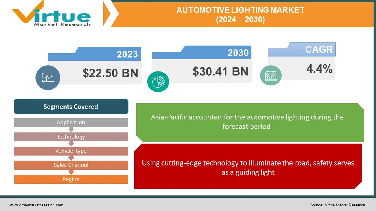
Global automotive lighting refers to all vehicle lighting systems, from headlamps that illuminate the road to taillights that communicate movements. They guarantee motorists and other road users alike safety, visibility, and style. While taillights frequently use LEDs for improved visibility, headlights are available in a variety of technologies, including LED and laser. Interior illumination, DRLs, and signal lights all have a role to play. This market, which was estimated to be worth $33.64 billion in 2022, is anticipated to rise to $67.39 billion by 2030 because of laws, luxury tastes, safety concerns, and technological developments like OLED taillights and adaptive headlights. Anticipate a future dominated by intelligent, connected, personalized, and sustainable lighting systems that enhance the safety, efficiency, and aesthetic appeal of automobiles.
Key Market Insights:
Car lighting works its magic to provide safety, visibility, and style. Headlights cut through the night, taillights express intent, and interiors shine with comfort. The billion-dollar global business is expected to rise due to consumer demand for high-end experiences, safer roads, and cutting-edge technology. Imagine dynamic messages being painted by taillights, headlights that adjust to the road, and interiors that customize their atmosphere. Driven by technological advancements like linked systems and laser beams, this future is calling. Anticipate even more visually attractive, environmentally friendly, and intelligent lighting to illuminate the way ahead, making cars safer, more efficient, and unquestionably cooler.
Global Automotive Lighting Market Drivers:
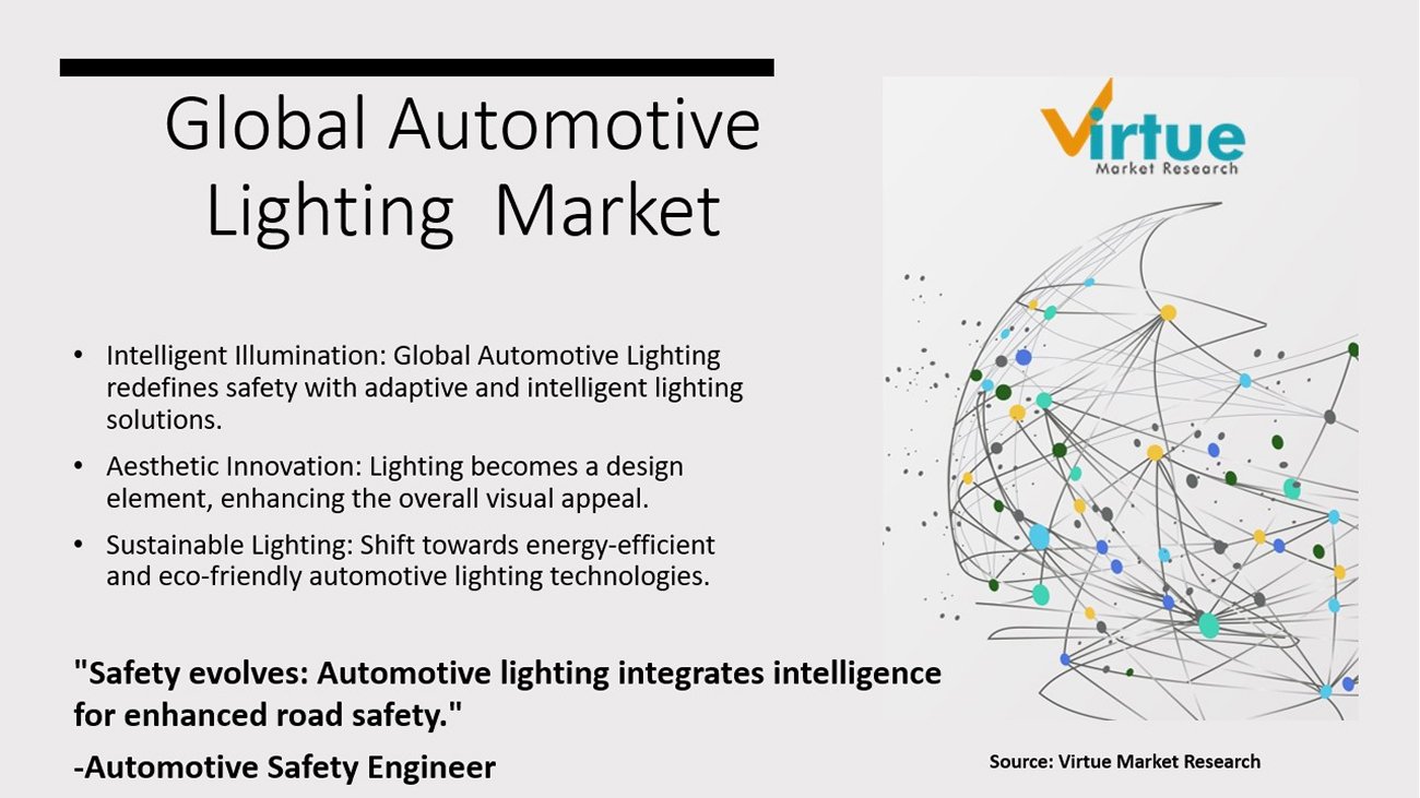
Using cutting-edge technology to illuminate the road, safety serves as a guiding light.
In the market for automobile lighting, safety is the driving force behind demand from the public and laws. While automated high beams smoothly react to traffic, adaptive headlights modify their beams so as not to blind other people. With visually striking displays, dynamic taillights convey intentions for braking and turning. Beyond these developments, integrated pedestrian identification and lane departure alerts will soon make roads safer and brighter for everyone.
Beyond Performance-Based Luxuries Redefined by Light.
Luxurious automobile lighting creates a distinct visual identity that goes beyond simple illumination. Personalized interior lighting customizes the driving experience by setting the mood with a range of colours and intensities, while intricate designs and distinctive DRLs modify exteriors. As you approach your automobile at night, welcoming lights lead the way, resulting in an interior that is perfectly lit. Not only is this symphony of light aesthetically pleasing, but it also stands as a tribute to luxury. Upcoming developments like gesture-controlled lighting and holographic displays promise to further enhance the experience.
Fuel Efficiency Takes the Lead: Illuminating Sustainability
The worldwide automotive lighting market is undergoing a significant transition towards energy-efficient solutions, as environmental concerns gain prominence. LED technology is leading the way, providing a ray of hope for the environment and drivers alike. LED lights beam brighter and use a lot less energy than conventional halogen lamps. There are some tangible advantages to this. For drivers, this translates to increased fuel economy, which lowers petrol prices and lessens reliance on fossil fuels. Greater air quality and a reduction in the transport sector's contribution to climate change are the results of reduced overall emissions.
To Learn more about this report,
Global Automotive Lighting Market Restraints and Challenges:
Although the global automotive lighting business is booming, there are still unknowns. Difficulties impede growth even as innovation propels it with eye catching features like laser beams and adaptable headlights. These technologies are luxury items due to their high cost and difficult integration, which puts producers' abilities to the test. The worldwide patchwork created by unclear legislation limits the potential of innovation. Durability issues persist, particularly when complex systems are subjected to challenging conditions. Ultimately, a lot of drivers still don't fully understand how these improvements can help them. Together, we can overcome these obstacles. The keys to reducing costs are improved production, more seamless integration, and unified regulations. Their full potential can be realized by educating customers about the safety, efficiency, and aesthetic value of these lighting wonders. By working together, we can pave the way for an even brighter and safer future for vehicle lighting.
Global Automotive Lighting Market Opportunities:
It is made possible by advanced LED technology, which gives drivers the ability to customize their illumination for the highest level of comfort and flair. Consumers that care about the environment want greener products, and vehicle lighting complies. While solar- and self-powered lighting technologies offer a future powered by clean energy, energy-efficient LEDs lower pollution. The advent of connected lighting systems heralds a new age. Envision automobiles interacting with infrastructure and one another to minimize accidents and enhance traffic efficiency. Integrated headlights with pedestrian recognition provide unmatched safety, while dramatic taillights with eye-catching displays alert onlookers to your intentions. The possibilities are endless in the future. Gesture-controlled interior illumination, holographic displays projected onto the road, and even light fixtures with self-healing capabilities.
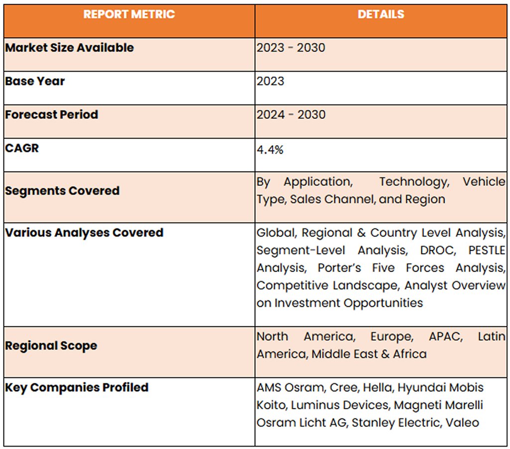
AUTOMOTIVE LIGHTING MARKET REPORT COVERAGE:
To Learn more about this report,
Global Automotive Lighting Market Segmentation: By Application
Exterior Lighting
Interior Lighting
Due to laws requiring safety features like headlights, taillights, and brake lights, exterior lighting presently holds the most market share in the vehicle lighting industry. The dominance of this market is partly attributed to advancements in safety-focused technologies such as adaptive headlights and daytime running lights. The market value of external lighting is increased by the quick adoption of technology like LED bulbs and laser lights, which improve performance and aesthetics. Conversely, the interior lighting market is expected to increase at the fastest rate in the upcoming years. Innovations like ambient lighting and technology breakthroughs like LED and OLED displays, driven by consumer demand for comfort and personalisation, open new possibilities. The spread of sophisticated interior lighting systems is further driven by the growing emphasis on safety and the expansion of the luxury car market.
Global Automotive Lighting Market Segmentation: By Technology
Halogen
LED (Light-Emitting Diode)
Xenon
Emerging Technologies
The worldwide vehicle lighting market is currently dominated by halogen because of its more affordable price, advanced technology, and useful illumination. With its dependable supply chain and affordable option for manufacturers and cost-conscious customers, halogen holds the biggest market share. The fastest-growing market right now is LEDs, which are predicted to shortly overtake halogen. The rapid expansion of LEDs is driven by their higher efficiency, longer lifespan, flexibility in design, and technological breakthroughs including enhanced brightness. Because LEDs use less energy and produce fewer emissions and better fuel economy, they are becoming more and more popular in the changing automotive lighting market.
Global Automotive Lighting Market Segmentation: By Vehicle Type
Passenger Cars
Commercial Vehicles
Passenger automobiles rule the worldwide automotive lighting market. The sheer number of passenger cars produced which surpasses that of business vehicles and fuels the need for lighting systems is the primary cause of this popularity. The growing demand for personal automobiles in developing nations is a result of rising disposable income, which in turn drives the rise of the passenger car market. The importance that consumers place on safety and aesthetics elements helps to drive market expansion. But in the upcoming years, the market for electric and hybrid cars is expected to develop at the quickest rate. The exponential rise of the worldwide electric car market, which is still expanding and shows no signs of slowing down, is what is driving this surge. Specialised lighting solutions are required since electric and hybrid vehicles have different lighting requirements because of their specific functionality and design aesthetics.
Global Automotive Lighting Market Segmentation: By Sales Channel
OEM (Original Equipment Manufacturers)
Aftermarket
Most lighting systems sold nowadays are sold by OEMs (Original Equipment Manufacturers), primarily because manufacturers pre-install lighting systems in new cars. But in the next years, the aftermarket is expected to develop at the quickest rate. This spike in demand for replacement parts, especially lighting systems, can be linked to several variables, one of them being the average age of cars. The industry is expanding because of consumers' growing desire to personalise their cars with aftermarket lighting upgrades such LED upgrades and decorative lighting. The availability and affordability of technologies like adaptive headlights and laser lights in the aftermarket, together with other advancements in lighting technology, are driving demand even more. Moreover, the growing market for electric cars (EVs).
To Learn more about this report,
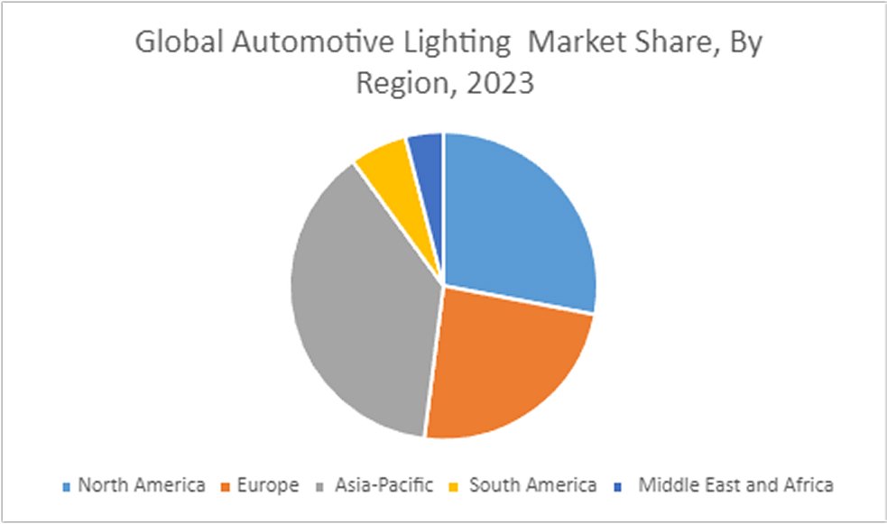
Global Automotive Lighting Market Segmentation: By Region
North America
Asia-Pacific
Europe
South America
Middle East and Africa
Throughout the forecast period, Asia Pacific is anticipated to be the automotive lighting market with the highest profitability. Over the past few years, Asia Pacific countries like China and India have seen notable increases in automotive manufacturing and sales, primarily in the medium-to premium luxury car segment. Asia Pacific is predicted to see an increase in the manufacturing of passenger cars, with India experiencing the strongest growth rate. Depending on the state of the national economy, the area offers a suitable selection of both high-end and cheap cars. For instance, there is a substantial demand for halogen, Xenon/HID, and LED since China and India produce more economy and mid-range automobiles. On the other hand, luxury car adoption rates are greater in South Korea and Japan, where LED lighting is the norm.
COVID-19 Impact Analysis on the Global Automotive Lighting Market:
A brief shadow was thrown by COVID-19 over the worldwide automotive lighting market. Production was stopped by lockdowns and supply chain disruptions, while luxury lighting upgrades were shelved by consumers on a tight budget. Resources became scarce, and R&D stagnated. Still, the market is recovering thanks to resurgent demand and rearranged priorities. While energy-efficient LEDs are being pushed towards adoption by sustainability, safety concerns are driving interest in features like pedestrian detection and adaptive headlights. The digital push of the epidemic creates opportunities for intelligent, networked lighting systems that may interact with infrastructure and other cars. Ultimately, the industry is positioned to shine brighter, focused on safety, sustainability, and a connected future, even though the pandemic dimmed its brilliance.
Recent Trends and Developments in the Global Automotive Lighting Market:
A development collaboration between OSRAM Continental and REHAU aims to incorporate lighting into external components, providing automobile manufacturers with innovative lighting options that improve functionality and design flexibility. For rear combination lamps, Hella unveiled a revolutionary lighting innovation called Hella FlatLight technology. A Memorandum of Understanding (MoU) was signed by Samvardhana Motherson Automotive Systems Group BV (SMRPBV), a division of Motherson Group, and Marelli Automotive Lighting to investigate a technology collaboration focused on intelligently lighted external body components. Valeo debuted their revolutionary 360° lighting system at the Shanghai Auto Show. This technology surrounds the car with a band of light, projecting instantaneous, clear signs that other drivers can see from a distance. Pedestrians, cyclists, and scooter riders are especially susceptible to these signals
Key Players:
AMS Osram
Cree
Hella
Hyundai Mobis
Koito
Luminus Devices
Magneti Marelli
Osram Licht AG
Stanley Electric
Valeo
Chapter 1. Gallium Arsenide (GaAs) Wafers Market– Scope & Methodology
1.1. Market Segmentation
1.2. Scope, Assumptions & Limitations
1.3. Research Methodology
1.4. Primary End-Use Industry `
1.5. Secondary Source Chapter 2. Gallium Arsenide (GaAs) Wafers Market– Executive Summary
2.1. Market Size & Forecast – (2026 – 2030) ($M/$Bn)
2.2. Key Trends & Insights
2.2.1. Demand Side
2.2.2. Supply Side
2.3. Attractive Investment Propositions
2.4. COVID-19 Impact Analysis Chapter 3. Gallium Arsenide (GaAs) Wafers Market– Competition Scenario
3.1. Market Share Analysis & Company Benchmarking
3.2. Competitive Strategy & Development Scenario
3.3. Competitive Pricing Analysis
3.4. Supplier-Distributor Analysis Chapter 4. Gallium Arsenide (GaAs) Wafers Market- Entry Scenario
4.1. Regulatory Scenario
4.2. Case Studies – Key Start-ups
4.3. Customer Analysis
4.4. PESTLE Analysis
4.5. Porters Five Force Model
4.5.1. Bargaining Power of Suppliers
4.5.2. Bargaining Powers of Customers
4.5.3. Threat of New Entrants
4.5.4. Rivalry among Existing Players
4.5.5. Threat of Substitutes Chapter 5. Gallium Arsenide (GaAs) Wafers Market- Landscape
5.1. Value Chain Analysis – Key Stakeholders Impact Analysis
5.2. Market Drivers
5.3. Market Restraints/Challenges
5.4. Market Opportunities
Chapter 6. Gallium Arsenide (GaAs) Wafers Market– By Wafer Type
6.1 Introduction/Key Findings
6.2 Semi-Insulating (SI) GaAs Wafers
6.3 Semi-Conducting (SC) GaAs Wafers
6.4 Others
6.5 Y-O-Y Growth trend Analysis By Wafer Type
6.6 Absolute $ Opportunity Analysis By Wafer Type , 2026-2030
Chapter 8. Gallium Arsenide (GaAs) Wafers Market– By Polishing Type
8.1 Introduction/Key Findings
8.2 Single-Side Polished (SSP)
8.3 Double-Side Polished (DSP)
8.4 Epi-Ready
8.5 Others
8.6 Y-O-Y Growth trend Analysis Polishing Type
8.7 Absolute $ Opportunity Analysis Polishing Type , 2026-2030 Chapter 9. Gallium Arsenide (GaAs) Wafers Market– By End-Use Industry
9.1 Introduction/Key Findings
9.2 RF & Wireless Communications
9.3 Photovoltaics & Space Solar
9.4 Photonics & Optoelectronics
9.5 LED & Display
9.6 Defense & Aerospace
9.7 Others
9.8 Y-O-Y Growth trend Analysis End-Use Industry
9.9 Absolute $ Opportunity Analysis, End-Use Industry 2026-2030
Chapter 10. Gallium Arsenide (GaAs) Wafers Market, By Geography – Market Size, Forecast, Trends & Insights
10.1. North America
10.1.1. By Country
10.1.1.1. U.S.A.
10.1.1.2. Canada
10.1.1.3. Mexico
10.1.2. By Wafer Type
10.1.3. By End-Use Industry
10.1.4. By Polishing Type
10.1.5. Diameter
10.1.6. Countries & Segments - Market Attractiveness Analysis
10.2. Europe
10.2.1. By Country
10.2.1.1. U.K.
10.2.1.2. Germany
10.2.1.3. France
10.2.1.4. Italy
10.2.1.5. Spain
10.2.1.6. Rest of Europe
10.2.2. By Wafer Type
10.2.3. By End-Use Industry
10.2.4. By Polishing Type
10.2.5. Diameter
10.2.6. Countries & Segments - Market Attractiveness Analysis
10.3. Asia Pacific
10.3.1. By Country
10.3.1.2. China
10.3.1.2. Japan
10.3.1.3. South Korea
10.3.1.4. India
10.3.1.5. Australia & New Zealand
10.3.1.6. Rest of Asia-Pacific
10.3.2. By Wafer Type
10.3.3. By Diameter
10.3.4. By Polishing Type
10.3.5. End-Use Industry
10.3.6. Countries & Segments - Market Attractiveness Analysis
10.4. South America
10.4.1. By Country
10.4.1.1. Brazil
10.4.1.2. Argentina
10.4.1.3. Colombia
10.4.1.4. Chile
10.4.1.5. Rest of South America
10.4.2. By Diameter
10.4.3. By Wafer Type
10.4.4. By End-Use Industry
10.4.5. Polishing Type
10.4.6. Countries & Segments - Market Attractiveness Analysis
10.5. Middle East & Africa
10.5.1. By Country
10.5.1.4. United Arab Emirates (UAE)
10.5.1.2. Saudi Arabia
10.5.1.3. Qatar
10.5.1.4. Israel
10.5.1.5. South Africa
10.5.1.6. Nigeria
10.5.1.7. Kenya
10.5.1.10. Egypt
10.5.1.10. Rest of MEA
10.5.2. By Wafer Type
10.5.3. By Diameter
10.5.4. By Polishing Type
10.5.5. End-Use Industry
10.5.6. Countries & Segments - Market Attractiveness Analysis Chapter 11. Gallium Arsenide (GaAs) Wafers Market – Company Profiles – (Overview, Portfolio, Financials, Strategies & Developments)
11.1 Freiberger Compound Materials GmbH
11.2 AXT Inc.
11.3 Sumitomo Electric Industries Ltd.
11.4 Wafer Technology Ltd. (IQE plc)
11.5 Vital Materials Co. Ltd.
11.6 China Crystal Technologies Co. Ltd.
11.7 Yunnan Germanium Co. Ltd.
11.8 Coherent Corp. (II-VI Incorporated)
11.9 Qorvo Inc.
11.10 Broadcom Inc.
Fill out the form below and our team will get back to you shortly
FAQ's
The primary growth drivers are the sustained global expansion of 5G wireless networks and smartphone RF front-end module demand, which structurally elevates SI GaAs wafer consumption through the proliferation of multi-band power amplifiers and LNAs per device.
The primary growth drivers are the sustained global expansion of 5G wireless networks and smartphone RF front-end module demand, which structurally elevates SI GaAs wafer consumption through the proliferation of multi-band power amplifiers and LNAs per device.
The most significant challenge is the structural supply chain vulnerability created by the geographic concentration of gallium raw material production in China, which accounts for the majority of global gallium output as a byproduct of aluminum smelting.
The most significant challenge is the structural supply chain vulnerability created by the geographic concentration of gallium raw material production in China, which accounts for the majority of global gallium output as a byproduct of aluminum smelting.
Freiberger Compound Materials and AXT Inc. are the leading independent GaAs wafer suppliers serving global RF and photovoltaic customers. Sumitomo Electric Industries commands significant share in the Japanese and space-qualified segments. Vital Materials and China Crystal Technologies represent the largest Asian production capacity.
Freiberger Compound Materials and AXT Inc. are the leading independent GaAs wafer suppliers serving global RF and photovoltaic customers. Sumitomo Electric Industries commands significant share in the Japanese and space-qualified segments. Vital Materials and China Crystal Technologies represent the largest Asian production capacity.
Asia-Pacific holds the dominant market share, underpinned by China’s position as both the largest GaAs crystal growth production center and the home of major RF front-end module fabs consuming SI wafers at high volume.
Asia-Pacific holds the dominant market share, underpinned by China’s position as both the largest GaAs crystal growth production center and the home of major RF front-end module fabs consuming SI wafers at high volume.
North America is demonstrating the fastest regional growth, driven by CHIPS Act-funded investments in domestic compound semiconductor substrate and device manufacturing capacity.
North America is demonstrating the fastest regional growth, driven by CHIPS Act-funded investments in domestic compound semiconductor substrate and device manufacturing capacity.
More related reports
Get expert-driven market research reports from a leading research partner to help you navigate the future of the global industry.
Report Code: VMR-19367 | Published Date: May 2026 | Format: Excel and PDF
As of 2025, the market was estimated to be around USD 410 billion, which took into account the cumulative investments, production, and development of the ecosystem associated with the localized production of semiconducto...
Report Code: VMR-19286 | Published Date: April 2026 | Format: Excel and PDF
In 2025, the global Nearshoring and Contract Manufacturing for Electronics Market was valued at approximately USD 759.93 billion. It is projected to grow at a CAGR of around 12.66% during the forecast period of 2026–2030...
Report Code: VMR-19221 | Published Date: March 2026 | Format: Excel and PDF
In 2025, the High-Temperature Electronics Market was valued at approximately USD 3.94 billion. It is projected to grow at a CAGR of around 7% during the forecast period of 2026–2030, reaching an estimated USD 5.53 billio...
Report Code: VMR-19228 | Published Date: March 2026 | Format: Excel and PDF
In 2025, the Semiconductor Probe Cards Market was valued at approximately USD 2.6 billion. It is projected to grow at a CAGR of around 7.2% during the forecast period of 2026–2030, reaching an estimated USD 3.68 billion...
Report Code: VMR-19218 | Published Date: March 2026 | Format: Excel and PDF
In 2025, the Semiconductor Wafer Handling & AMHS Market was valued at approximately USD 6.2 billion. It is projected to grow at a CAGR of around 8.6% during the forecast period of 2026–2030, reaching an estimated USD 9.3...
“We received a complex piece of work for our niche market from Virtue Market research in short period of time. I appreciate the quality and content of the final files we received. Thanks for the support”
Medical Devices Company based in Europe
“We received a complex piece of work for our niche market from Virtue Market research in short period of time. I appreciate the quality and content of the final files we received. Thanks for the support”
Medical Devices Company based in Europe
“We received a complex piece of work for our niche market from Virtue Market research in short period of time. I appreciate the quality and content of the final files we received. Thanks for the support”
Medical Devices Company based in Europe
“We received a complex piece of work for our niche market from Virtue Market research in short period of time. I appreciate the quality and content of the final files we received. Thanks for the support”
Medical Devices Company based in Europe
“We received a complex piece of work for our niche market from Virtue Market research in short period of time. I appreciate the quality and content of the final files we received. Thanks for the support”
Medical Devices Company based in Europe
“We received a complex piece of work for our niche market from Virtue Market research in short period of time. I appreciate the quality and content of the final files we received. Thanks for the support”